Comparison of Sleep Currents for XIAO ESP32C6, S3, and C3

Now that I have three different XIAO ESP32s (C3, S3, and C6), compared their sleep currents. I hope this will be helpful when considering low-power applications.

First, I analyzed the schematic and datasheet as a reference.
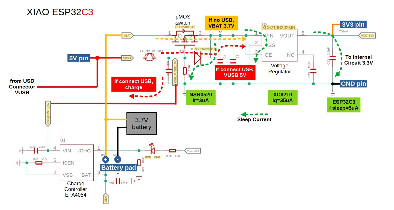
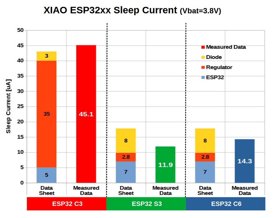
A 3.3V analog regulator XC6210 is used in C3, and this regulator’s quiescent current of 35uA accounts for most of the C3 sleep current. However, a diode NSR0520 is used, which has low reverse current, giving it an advantage in this area compared to S3 and C6.
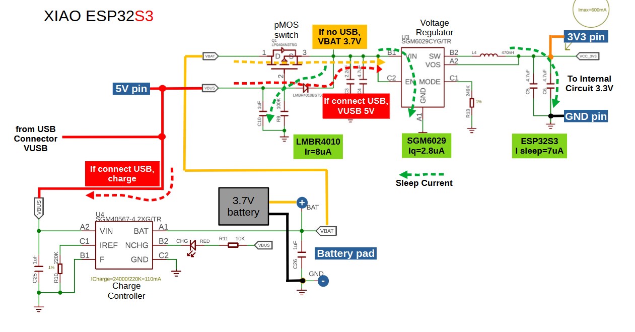
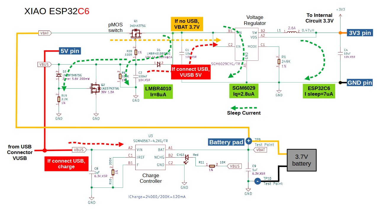
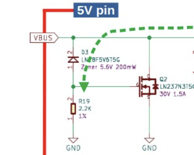
The power supply circuits for S3 and C6 are almost identical. The 3.3V regulators in S3 and C6 are SGM6029 with power save mode, resulting in a much smaller sleep current of 2.8uA. Unfortunately, the diodes have been replaced by LMBR4010, which have a large reverse current of 8uA and account for half of the sleep current in S3 and C6.

EDIT : A mistake was found in the measured sleep current of C3, which has been corrected.

The following sketch was compiled and used for the measurements, with options in default state.
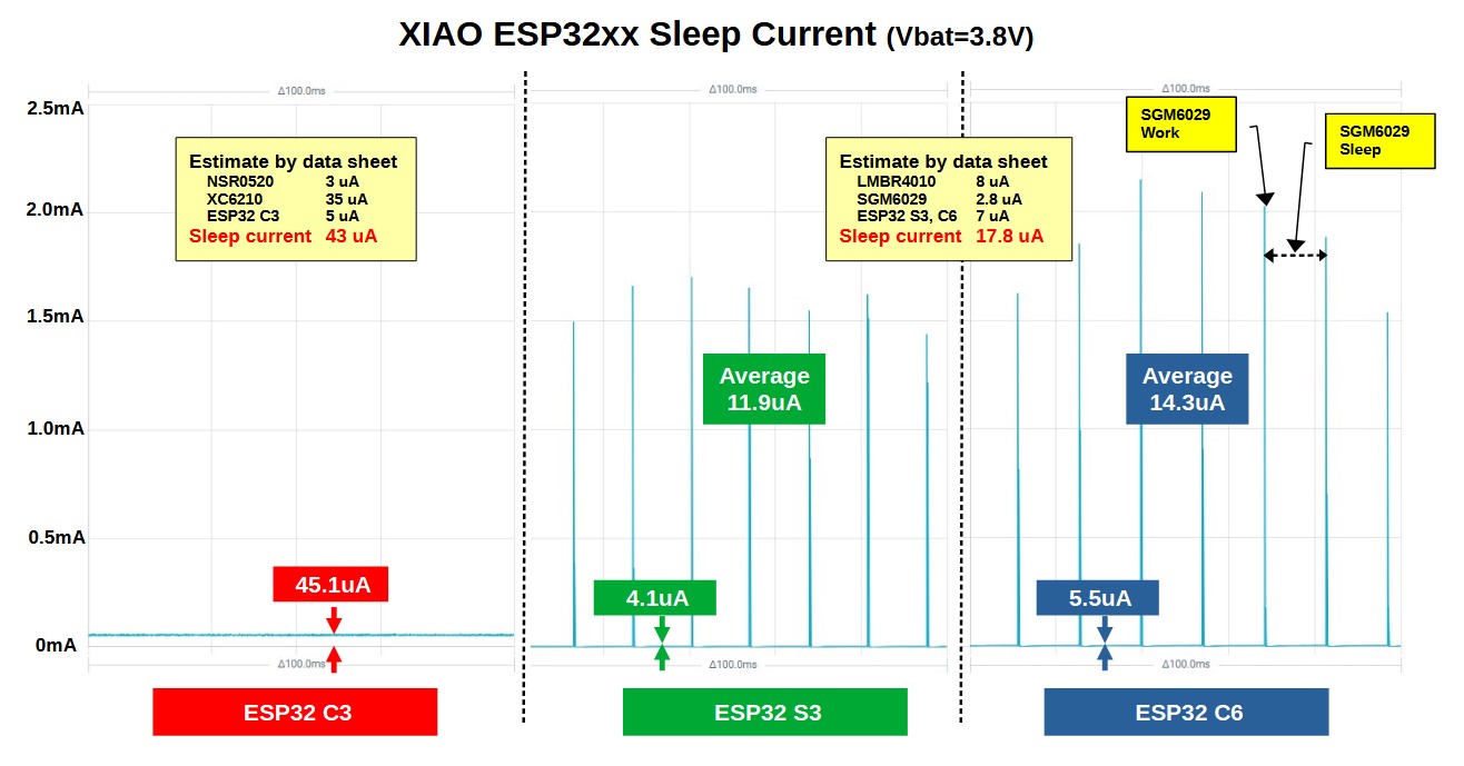
Sleep current was measured by applying 3.8V from PPK2 to the battery pad.
Since a diode is sensitive to temperature, I thought I measured at a constant room temperature for comparison purposes, but it was difficult to achieve a strictly constant temperature. Measurements may have been affected by temperature. The current waveforms of S3 and C6 show the power save mode of the regulator SGM6029 at work. C3 was 45.1uA, S3 was 11.9uA, and C6 was 14.3uA.

// Board Library : esp32 by Espressif 3.0.0-rc1
// Board Select  : XIAO_ESP32C6, XIAO_ESP32S3, XIAO_ESP32C3
// ArduinoIDE compile options left at default
// Vbat = 3.8V

void setup() {
  esp_deep_sleep_start();
}

void loop() {
}

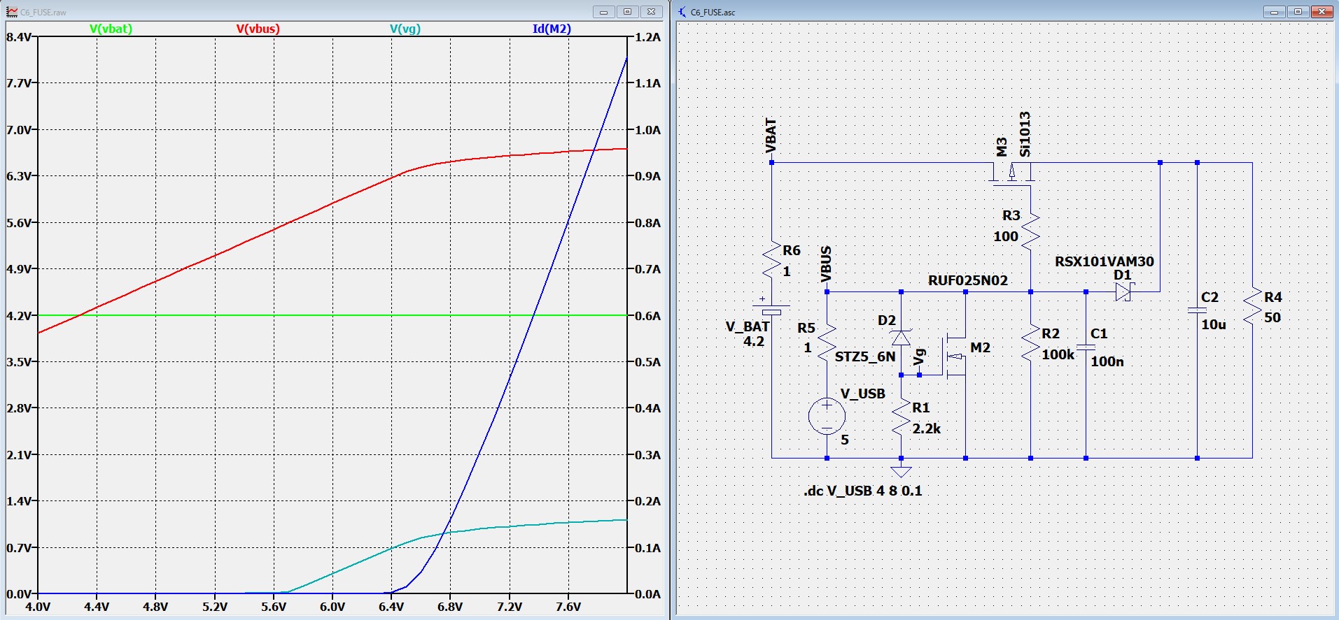
The power circuit section of each XIAO are listed for reference.

8 Likes

Impressed I am.

Heaps of useful info.

There was an error in the measured sleep current for C3, so the graph and values in Post 1 have been corrected.

didnt someone say somewhere that you can measure battery voltage in software by using the bluetooth/wifi subsystem… i saw that somewhere but lost it

Hi there,
Awesome as per usual with the Power Nija :ninja: I don’t see the usefulness of the C3, always felt like it was the red headed step child, The S3 is the “Shazzizle’my-nizzle” :dog2: imo. I/O for days B2B connector and Power sipping through a straw, smooth.
I won’t pull a c3 out for anything unless it’s on a grove expansion board with the added flash chip installed.
C6 is still getting the treatment. so stay tuned.
GL :slight_smile: PJ

I would say no @cgwaltney on the BLE radio doing and Battery diags, there is a software battery gauge library , kinda smoke and mirror perfect world stuff IMO, based on internal battery resistance etc.
:v:

Hey!

That is really impressive detective work there. I am looking at the ESP32C6 circuit and there is this part:

It looks like some over voltage protection? but it is weird because the MOSFET source is connected to ground. Does anyone know what this part of the circuit does? (sorry if this is a noob question)

Hi there,
I’ll bite, Looks to me as if the USB is connected the small voltage bias provided by the Zener Diode is pulled lower and Shuts down the path to GND for the 3.3v path.
With out it (usb) plugged in then the mosfet is able to sync the current and complete the path to GND.
my .02
Others can comment on more.
HTH
GL :slight_smile: PJ
:v:

interesting… it seems the Z diode on the 5v power pin has been a frequent question…
Shame we only have ammiture engineers on this thing…

I smoked my first one back in the late 70’s , you never forget. :face_with_peeking_eye:

I like it doesn’t act like a diode until it breakover voltage

Hey whats an “ammiture”? :thinking: and can you elaborate more on how does one feel after smoking a diode, i may want to try it. Thanks!

1 Like

lol… its that part inside an electric motor that goes arround… I cant spell my own name… stupid AI can tell me that its spelled wrong… but not enough smart to tell me the right spelling… worse than an iPhone… What Da?

1 Like

Hi there,
Kinda the same It smells , your eyes get all glassy and the radio stops working completely…
Freaking you out… :woozy_face: :dizzy_face: :partying_face: :drooling_face:
HtH
PJ :slight_smile: GL
:v:

Thanks for the explanation, and for the great laughs. Have a good weekend

1 Like

We’re here all week…LOL U2 :v:

Looks the circuit is intended to short VBUS, which presumambly has a current limit or fuse, in the event of VBUS being maybe 6V or a bit more.

The zenner is only 200mW, so thats not able to absorb much power before melting, but when the MOSFET turns on it can handle 1.5A.

1 Like

Yes that is what i thought, but can you explain why the mosfet source is connected to ground, and the drain to VBUS… will it short VBUS to GND when the gate is open? it looks like the mosfet should be connected the other way around. but pls note i am an “ammiture”

Does the schematic show a P-Channel or an N-Channel MOSFET ?

schematic shows LN237N3T5G which is Single N-channel Trench MOSFET

Hi StuartsProjects,
The simulation using LTspice gave results that support your idea. The device models are similar and may not be accurate, but I believe it represents the behavior of the circuit qualitatively.
If you are interested please run the attached file.

C6-FUSE.zip (236.3 KB)

3 Likes

Thanks for taking the time to simulate the circuit. However, can you confirm your m2 mosfet is connected in the same orientation as the xiao esp32c6 schematic? LTspice does not annotate drain and source so i cannot tell. The original circuit has the mosfet source connected to ground, and the drain to VBUS.