Hello. I’m frustrated that there is no schematic for the actual wio-sx1262 module. The bogus link “WIO-SX1262 Schematic” is basically a “wiring diagram” of their XIAO “ hat, which helps NO-ONE actually trying to use the module!!
To actually use this part in a real design, I need to know EXACTLY how the pins brought out of the module are connected to the SX1262, specifically the what the RFSW pin is, i.e., did Seeed follow the Semtech ref design and use a PE4529 rf switch? Have they connected DIO2 to the CTRL of the switch and connected the exported RFSW pin to the PE4529 /CTRL pin? We need to know this stuff!!! Come on Seeed!!!
HI there,
So, I’m not feeling it, 
They have all the documentation in the WiKi…
The link you posted is from the sensecap ? hardware AFAIK , the schematic is there and it is the same as the reference design in the Data-sheet , pg12?
If you want what is under the CAN, ? That’s not going to happen…  Proprietary, like the code.
They have two different daughter boards with it, one for esp32S3 (B2B) and one for Nrf52840 (SPI)
Which device are you having issue with ?
HTH
GL  PJ
PJ 

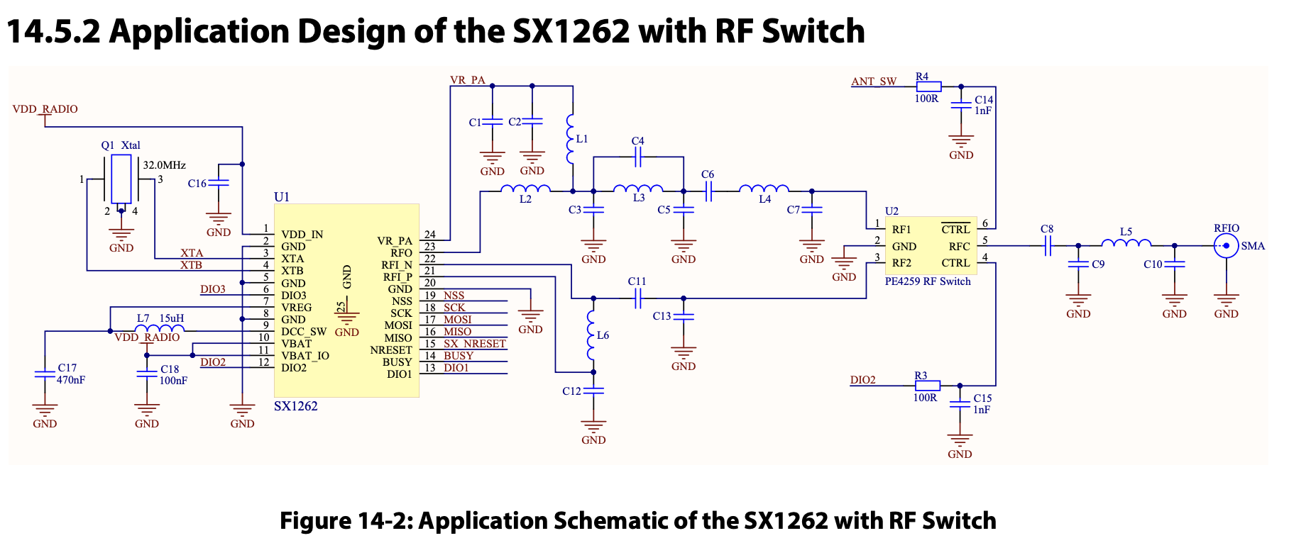
Thanks for responding. I’ll stick with the issue I’m having as opposed getting into a “what’s proprietary in a reference design.” We’re paying for the tuning of the rf circuitry on the module pcb - otherwise we’d just use the sx1262 directly. The issue is the RFSW pin from the wio-sx1262 pin lack of explanation. In the Semtech LORA stack, using their ref design:
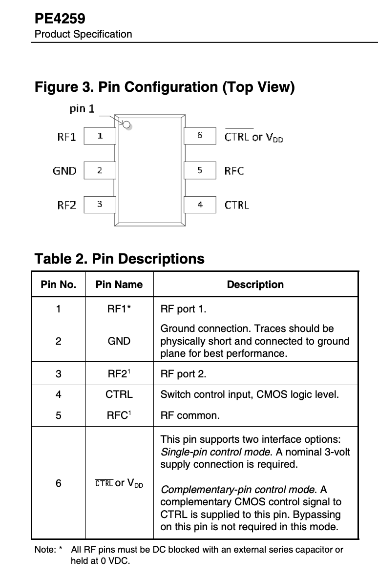
you can configure DIO2 to control the RF switch, eliminating the need for an extra GPIO (and cycles) from the uC. This is based on using the ref design using the very common PE4259 rf switch - It has 2 CTRL pins:
Some hint as to how they’ve connected DIO2 internally, aka, some text or a flippin schematic, with TBDs instead of actual component values, if you like, would be killer dude!
Hi there,
OK, Now we are getting somewhere… Very good explanation BTW. 
So , I assume You have pend this exact concern and verbage to [email protected] team? I’m Glad You  get the proprietary part and the need because of the competition in the small space(getting wider)
I would say ALSO pin 6 is of big concern and understanding the two modes of possible operation.
Some of the other LORA wizards present on here, can comment. I would think if you agree to a seeed NDA they could let you peek at the section of the schematic you need to make Proper engineering production decisions, component selection, etc. and costs. 
I’ll mention it, in next interaction I have with the Seeedineers see if they can’t hold a flash light or something
HTH
GL Pj
You may want to run (email) a design file past the Seeed Fusion service…never know what you can learn as well as the costs.
(only as an avenue of investigation)
I think that the information on the RFSwitch is in the datasheet? Not the actual rf switch device used, but the connection of DIO2 internally to the switching device select pin.
Perhaps you could have another look at the datasheet before contacting Seeed support?
Hi there,
Send the inquiry, there is nothing in the data sheet that will tell which path they chose AFAIK…  We can guess but that won’t do it. PIN 6 is an unknown (on the ref switch) how it is handled in Software. Fair question IMO.
I would think the AUTO mode would be a default option, only because as You indicate eats up cpu cycles unnecessarily if done the other way.
Well keep looking
GL PJ
I’ve sent an inquiry - I’ll post the response
Hi there,
Awesome, I also sent Kevin Y. a DM and forwarded our discussion link.
Start the timer
You probably know the New Lora chip is out also, I bet a BAG  they are working on something, No more seperate chips for EU and US is Great!
Key features of the LoRa Plus™ LR2021 include:
- Terrestrial and NTN, sub-GHz, 2.4 GHz ISM bands and licensed S-band radio
- Multi-PHY compatibility enables LP wireless protocols with third-party stacks
- FLRC up to 2.6 Mbps, LoRa up to 125 kbps, FSK, OOK, O-QPSK and LR-FHSS modulations
- Multi-region operation with single switch-less front-end design
- +22 dBm to -10 dBm Transmitter, offering best-in-class energy efficiency
- Multi-SF Receiver with low noise figure, Improved CAD and best LoRa sensitivity down to -141.5 dBm @ SF12/125 kHz
- Increased frequency offset tolerance obviating TCXO and large thermal relief
Year of the Fire Horse …
So I say let’s kick some ASCII
GL PJ
Good luck with the response from Seeed support.
This post may be of some assistance while you’re waiting.
RF_SW is connected to CTRL2 (pin 6) of the RF Switch.
DIO2 is connected to CTRL1 (pin 4) of the RF Switch.
I tend to connect RF_SW high (VDD) and let the library/chip handle the RF Switch control via DIO2
Hi there,
Sorry for the inconvenience and frustration this may cause. The internal wiring of the wio-SX1262 module follows the Semtech ref design: the DIO2 is connected to CTRL(pin4); the RF_SW is connected to /CTRL(pin6) of the RF switch, and this IO controls the working mode (set RF_SW HIGH enables the receiver mode).