Hi,
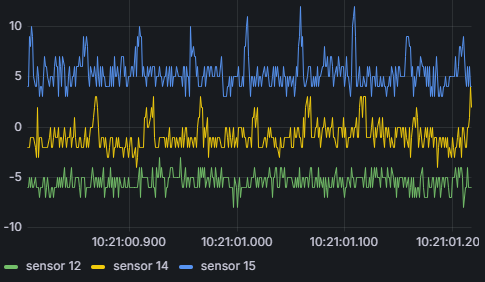
I am developing BLE sensors and after working with the nRF54L15DK boards, I have now bought 5 XIAO boards to integrate everything in a smaller form factor. With these boards I noticed that I have noise in my ADC readings, which corresponds to the BLE connection interval (50 ms in my case, but I have chagned it and the noise changed accordingly). The attached image shows the values sampled at 1 kHz with 3 different XIAO boards, using AIN2 and AIN3, which were shorted together on the header. I have tried different combinations of TACQ and TCONV but they don’t any effect on this noise.
Interestingly, some boards show less noise, but FFT analysis confirms that the noise is present in all of them. FFT analysis of the DK boards shows no such noise at all (at 20 Hz/50 ms the signal is in the noise floor). I have even tried swapping the nRF54L15 chip from a XIAO board with low noise to a board with high noise and the noise stayed with the board not the chip, though they both changed a bit, so it seems to be a board design issue rather than a faulty chip.
Could someone at seedstudio confirm my observations and maybe suggest a fix?
Thank you and best regards
Sašo
If you could show us your setup—and ideally your code—someone else could reproduce the issue.
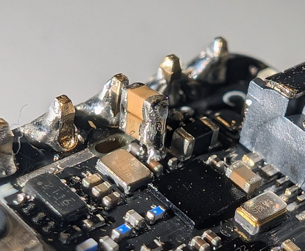
Here is a minimal example to reproduce the problem. The code acquires 1024 samples at 1 kHz every 10 seconds and sends them out the serial port. The hardware setup is simply a XIAO nRF54L15 with the pin headers soldered on and a jumper between pins D2 and D3 (AIN2 and AIN3).
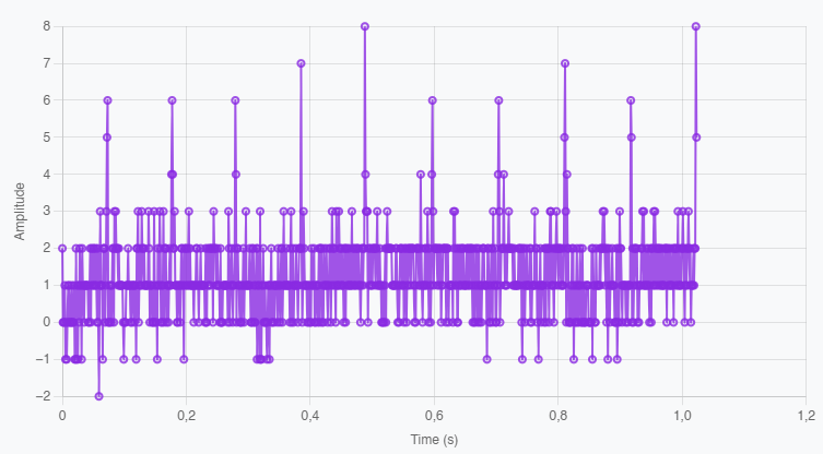
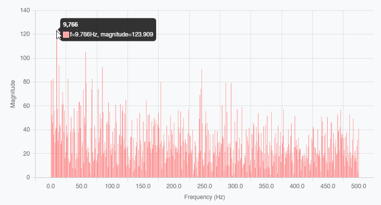
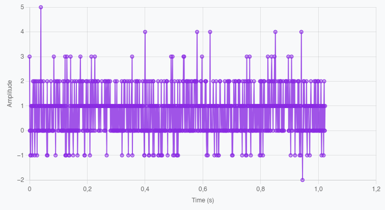
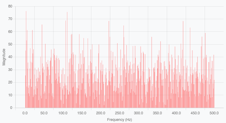
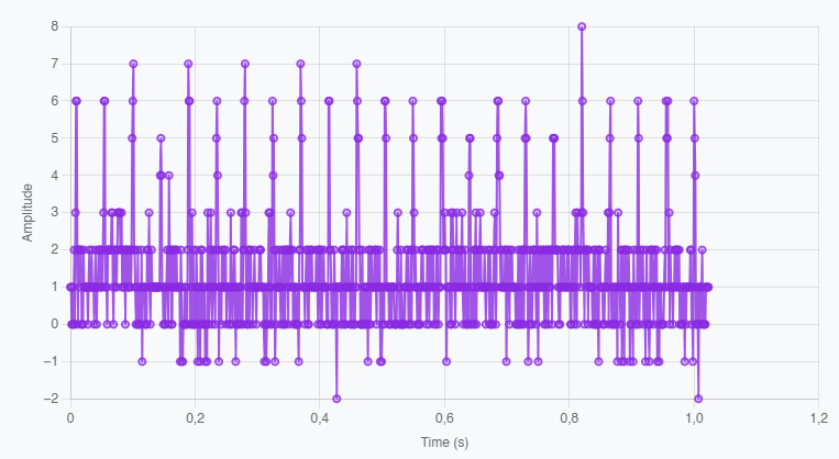
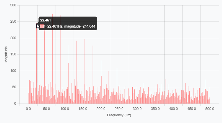
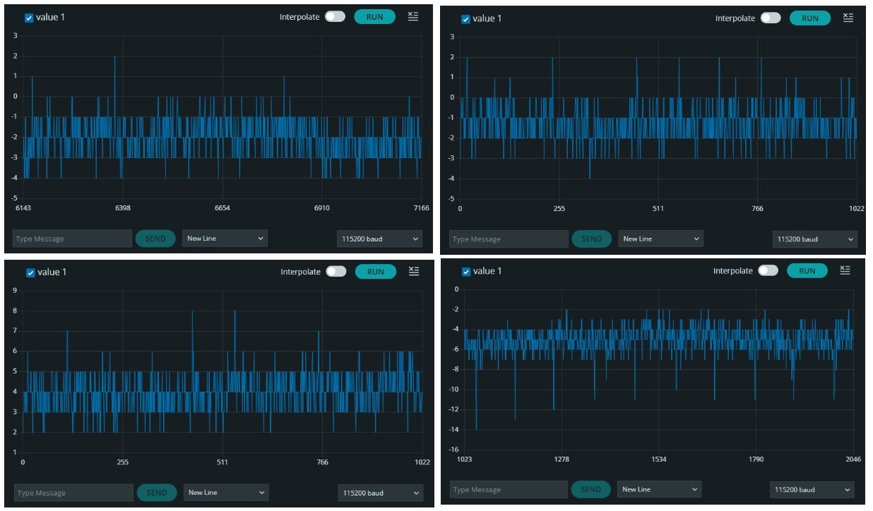
After uploading the code to the XIAO, it will start advertising, at this point if you take the samples from the serial port and run an FFT on them you will see that there is noise at around 10 Hz (the advertising interval is around 100 ms). Then you can connect using nRF Connect. At this point if you do FFT on a fresh set of samples, the noise will be basically gone. This is because there is almost no communication going on (the connection events are very short). Then you can subscribe to notifications on the Unknown Characteristic in the Unkown Serivce and the board will start streaming some data. Now if you do FFT on the samples you will see a lot of noise with the period equal to the connection interval (45 ms in my case). In my cases the signals look like this:
Advertising:
Just connected:
Connected and streaming data:
In this case FFT isn’t even needed, but for other boards I noticed that the noise was still there but around the level of the rest of the ADC noise, so not that noticeable or problematic.
I used this website for the FFT, setting FFT size to 1024 and sample rate to 1000 Hz.
adc_test.zip (2.8 KB)
Hi there,
And Welcome Here…
So those are interesting findings, Can you post a picture of the DUT ?
and the code you used to determine those indices. 
Are you removing the CAN and replacing it each time ?
Thank you for the contribution.
HTH
GL  PJ

Why the DK Board Passes: The nRF54L15 Development Kit has a ground plane layout, dedicated power regulation stages, and bulk decoupling explicitly engineered to isolate the RF section from sensitive analog domains. A small XIAO form factor board packs the antenna, matching network, and microcontroller pins into a tiny footprint, making it much harder to maintain pristine isolation.
Some observations,
The Xiao has one situation that can’t be overcome physically (SIZE) therefore , we can try adding a LAGRE bulk Capacitor or A combination of a 1uF and a smaller $0.1uF ceramic capacitor (X7R dielectric) placed as close as humanly possible to the VDD and analog reference pins helps shunt high-frequency transients to ground before they skew the SAR ADC’s sample-and-hold capacitor array.
Please try that on a new UN-touched Xiao as a reference,
and report back. 

I removed the shield on two of the 5 boards, so I could do the swap. I have not put it back yet, but didn’t find much difference between the signals before I removed it and after I removed it. The noise didn’t get worse.
Hi there,
So could you solder them, or isolate them at all?
The Jumper Wire Antenna Effect: Using a loose jumper wire between D2 and D3 (AIN2/AIN3) without proper shielding or twisting can turn that wire into a makeshift loop antenna, picking up 2.4 GHz RF energy radiating straight off the XIAO’s onboard trace antenna during BLE bursts and rectifying it into the ADC channel.
How are you powering the setup , & DUT ?
USB Power Rail Resonance: If You’re powering the board directly from a PC USB port or a cheap switching wall brick while pulling serial debug logs at 1e3 samples/sec, the shared ground return and dirty VDD rail can inject high-frequency switching noise right into the internal reference.
I have seen that web FFT before…
Sampling vs. Event Aliasing: Running a fixed 1 kHz software sampling loop while the Bluetooth stack is asynchronously handling background radio events can create weird beat frequencies or aliased artifacts in the FFT that look like structured noise, even if the raw analog signal is relatively clean.
Something to consider, try to mitigate with the Added Capacitance.. IMO, should fix it ALL up. 
HTH
GL PJ
Hi there,
Very interesting , “No effect” Hmmm, that’s not right. 
Something else then…?
Great work , good stuff.
Keep going.
GL PJ
I would like to see the nRF52840 in this test ?
Thanks for the suggestions, I will try to add the VDD/VREF capacitors tomorrow, this seems like it could help the most.
By jumper I meant the small jumpers that go directly on pin headers so I think it shouldn’t pick up too much RF noise. But I can also try putting a solder blob directly across the pins.
The power has been both USB and battery, the noise was present on both.
In my actual project code I have the sampling triggered via PPI from the GRTC so clock jitter shouldn’t be a problem.
Unfortunately I do not have a XIAO nRF54820 to compare. I do have XIAO nRF54LM20A.
I will report tomorrow with more findings.
Hi @sasodoma, I have a few questions.
- What is the purpose of connecting the two ADC input pins? Are there two input signals? Or is this a differential input?
- Even if it is a differential input, low-impedance signal sources are generally connected to the inputs—so what is the point of testing without connecting anything?
- Is the ADC’s Vref set to VDD (3.3 V), or is it the internal reference voltage of 0.9 V?
- Since the ADC is used to measure RSSI, this might have an effect. What would happen if we stopped measuring RSSI?
- The XIAO has an RF switch for selecting the antenna, but transmitting without an antenna may cause significant noise.
Hi, thanks for the reply.
- Yes I forgot to mention that, this is a differential input
- The ADC normally measures a current shunt but I have shorted the pins directly to verify that the noise is not coming from the outside. This is a minimal setup to reproduce the problem that I’m having. I have also tried shorting the pins together and connecting them to ground to make sure they are not floating. The result was the same.
- I believe the nRF54L15 only supports Vref to be 0.9V ± 5%. The reference is set to the internal one.
- Does the RSSI measurement run by default? I’m not using that functionality in my code.
- I have the switch set to the default value, which is the onboard ceramic antenna. I will try using the external antenna to see if there’s a difference.
If the ADC input(A1, A2) is connected to GND, won’t the conversion result be zero?
I’m not running the ADC and Advertising in a multitasking environment, but in my sketch, the reading is almost always zero.
I’m trying out your project, and while I can compile and upload it, it doesn’t run—I get a BUS_FAULT error.
.
I see you’ve selected a ceramic antenna, but have you turned on the power to the RF switch?
EDIT:
I managed to get it working. The values displayed on the serial monitor are indeed not zero and vary significantly. Based on an analysis of the ppk2 current waveform, it appears to be performing an AD conversion and Advertising every 445 ms—is this correct?
I’m curious to see what happens if you switch the AD conversion from burst mode to one-shot mode.
Yes ideally the conversion result would be zero but of course there is an offset, some random noise and there is also BLE noise visible, which is what I’m asking about in the first place.
The advertising settings are BT_LE_ADV_CONN_FAST_2, which should be between 100 and 150 ms interval, this matches what I’m seeing on my phone in nRF Connect app. Then when I connect and subcribe to notifications, the connection interval is set to 45 ms.
The ceramic antenna is the default selection and the RF switch also defaults to on in the device tree config. I have previously also thought that this may be a problem so I checked the device tree.
Right now I am at work and have two unmodified XIAO nRF54L15 boards in front of me. I flashed the same code on both of them and shorthed the ADC inputs by twisting a bit of wire through the holes and cutting it off so it’s really short. One of the boards has no visible noise in the results even when streaming data via BLE (no noise is visible even in FFT), the other one has a lot of BLE noise. This is similar to the other two boards where I swapped the chips previously. Though in that case one board had a little noise (only visible on FFT) while the other had a lot of noise. It seems to me that there must be some kind of subtle difference between the boards since they are running the same code, the config can’t be the source of the problem.
I will try to add capacitors to VDD and Vref to see if that helps. Though I see that the KiCad project on the Wiki is outdated so the PCB layout isn’t the same.
Does this mean that there are some XIAO_nRF54L15 units that have issues and others that don’t, even when running the same code?
P.S.: It seems your code still doesn’t work on my XIAO. I’m getting BUS_FAULT and MPU_FAULT errors.
It seems to be more of a spectrum, where some work great, some are worse and some are really bad.
With regards to compiling, I’m not sure what else can be done. I can send you my hex file if you are able to flash it directly.
It is flashed with:
openocd.exe -s 'C:/ncs/v3.4.1/zephyr/boards/seeed/xiao_nrf54l15\support' -s C:/ncs/toolchains/4f5b6ad6dd/opt/zephyr-sdk/hosttools/openocd/share/openocd/scripts -f 'C:/ncs/v3.4.1/zephyr/boards/seeed/xiao_nrf54l15\support\openocd.cfg' '-c init' '-c targets' -c 'reset init' -c 'nrf54l-load C:/Users/User/Documents/nRF_Projects/adc_ble_noise_test/build/adc_ble_noise_test/zephyr/zephyr.hex' -c 'reset run' -c shutdown
zephyr.zip (141.8 KB)
As an update, I have soldered some “massive” 0603 capacitors to the filtered supply rail (DECA and DECRF pins) the capacitors are 0.1 uF and 1 uF X7R. The noise did not get reduced by this.
I just accidentally took a deep dive into how the ADC works and there are capacitors and frequencies involved in the sensing operation… FYI
Fast forward to 1:55 +/-
Hi there,
Solid Work, my Guy
I believe you are on to it,  the PCB layout must have been revised, same code should give very close same results, sure could be some drift or noise, but NOT that BLE interference though, no way… You look at the DK schematic ? I bet they tweaked it for a component shortage or something and in there lies the rub, IMO
 and no-one checked. Let’s see, I want to loop in a Seeedineer and see if they can offer and pertinent info.
the attached ZIP is the file still being used to test with , give some more on the build please?
Toolchain , versions etc. the full Monty of your dev system and setup Please
we can get this figured out.
GL PJ
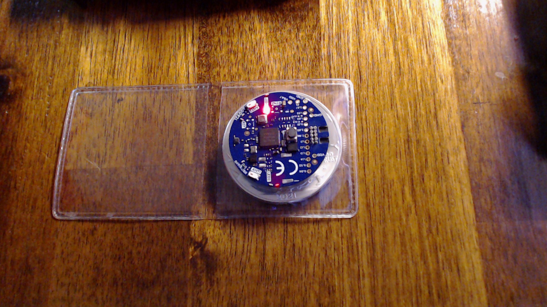
P.S. can you Post pic’s of front and back photo’s of these two Xiao devices ?
I don’t use ADC’s in m|y PCB’s or security Device so I’m good, but anything messing with my BLE gives me concern and is worth investigating.
Hi there,
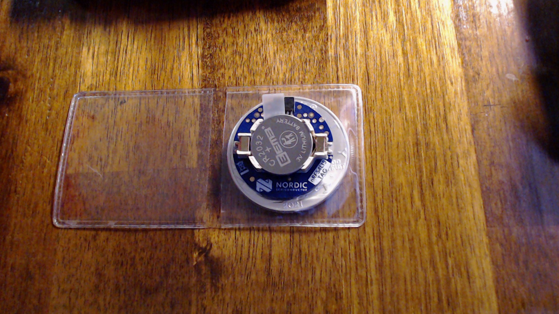
So , I want to try it on the “TAG”
Might give some good info on the schematic as well.
Time permitting , I can try to build it and flash it to the TAG
also can you post what serial output you expect?
HTH
GL PJ v:
Pressure washing my driveway so I’ll be in and out until later.
Hi there,
Can you try this and report back , Please
Isolate the RF Path (Radio Off vs. Radio On)
-
Disable the TX Power/Radio: Temporarily disable the BLE stack initialization entirely or use a firmware build where the radio initialization is skipped, but the ADC is run under the exact same timing loop.
-
If the noise completely vanishes with the softdevice/stack muted, it confirms the coupling is explicitly electromagnetic or supply-droop induced by the 2.4 GHz TX/RX bursts rather than generic ambient line noise.
HTH
GL PJ
or this one too,
Synchronize or Dither Sampling
- As
msfujino hinted at by mentioning burst vs. one-shot mode: try shifting the ADC acquisition to a timer-triggered one-shot mode decoupled from the radio events, or conversely, intentionally sync/phase-lock your sampling window away from the active connection/advertising slots. If continuous burst sampling is aliasing the 45 ms intervals, offsetting or changing the sample rate will drastically alter the noise signature.
FYI, I reached out to the MAIN MAN… Someone is coming. stay sturdy
It seems there was an issue with “west flash,” but when I programmed it using JLink, it worked without any problems.
Below are the ADC results obtained from four XIAO_nRF54L15 devices. It appears to be converting at 14-bit resolution, but I think this level of offset and noise is fairly normal. What do you think?