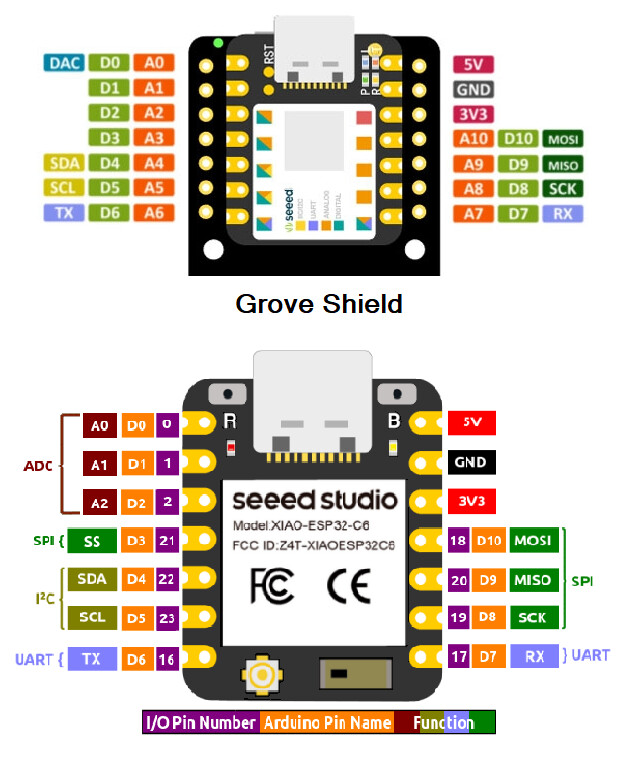
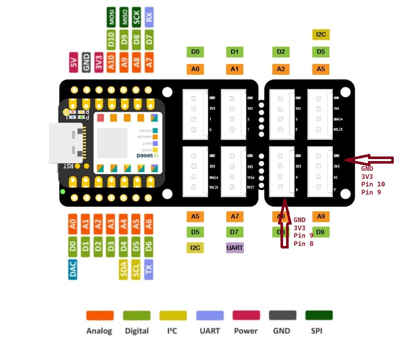
I’m trying to understand how the pins work with the shield. For example, on the grove shield, it says that one group of pins in GND, 3V3, 10, and 9. On the wiki page, it says that these are A9 and D9. However, the wiki for the esp32c6 doesn’t not show an A9 pin.
I tend to stick with the actual GPIO numbers for the ESP32’s, so D9 is GPIO_NUM_20 (in Arduino) and not an analog capable pin for ESP32-C6 - hence no A9 reference.
So there are “Silkscreen” pinouts Vendors use.
Programmers use the GPIO’s for code , UNLESS…!
The Boards support package .a.k.a. BSP include PIN macros that translate the SilkScreen numbers to GPIO’s, very processor specific. As @grobasoz indicates , stick with the GPIO’s You can’t go Wrong.
If I may..
PIN 9 is PIN 9 everywhere. it’s on multiple connectors, one could be part of the SPI interface connection (MISO(9), MOSI(10)), the other can be used for direct addressing or Vice-versa, just code it properly.
BTW , that silk screen colors squares is stupid confusing. but only for the mechanical connections, they did try to make a lot of options. USE the pin numbers on the board and the GPIO’s on the Code.
HTH
GL PJ
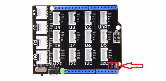
also , the adding external flash to Grove Expansion Board, Post may be of use.
relating , display, buzzer, button , sleep and Wake code to connections Helpful.
If i may add…. it is a little confusing that they call it D1 and A1… the important part is the 1… the meaning is this pin is in location 1 on the physical board…the only meaning is all pins are on a basic level digital (D) meaning they accept or output a digital signal… meaning 0V0 or 3V3 low or high
I call it the Physical Pin, or Board Pin number… as opposed to what I call the Logical Pin or the Chip Pin #… it is confusing, but to make it simple, each board has a pin, but each chip has a GPIO and depending on the chip used on the device, the logical pin may be connected physically on the board to a different physical or board pin… this is confusing but it happens when different chips need to be connected for different reasons that i dont understand
(A) Analog pins mean they can accept or output an analog signal, meaning the pin has access to an analog to digital converter… menaing if properly setup the pin can accept or output a proportional voltage at either 8, 10 or 12 bit resolution depending
(it is important in the setup code to assign ADC to pins to enable this feature)
to understand better, chips have ADC converter sub-systems, these sub-system units can be logicly connected to other elements to perform functions… if the code is incorect, the logical pipeline is corrupted… hope this is understandable
Most pins are digital by default… if you want it to perform analog functions, you have to assign it an analog resource units (ADC or DAC hadware)… this is done thru software configuration options
most pins can be A or D so it is assumed, but depending on the hardware, this may or not be true
alot of configuration options need to happen under the hood….
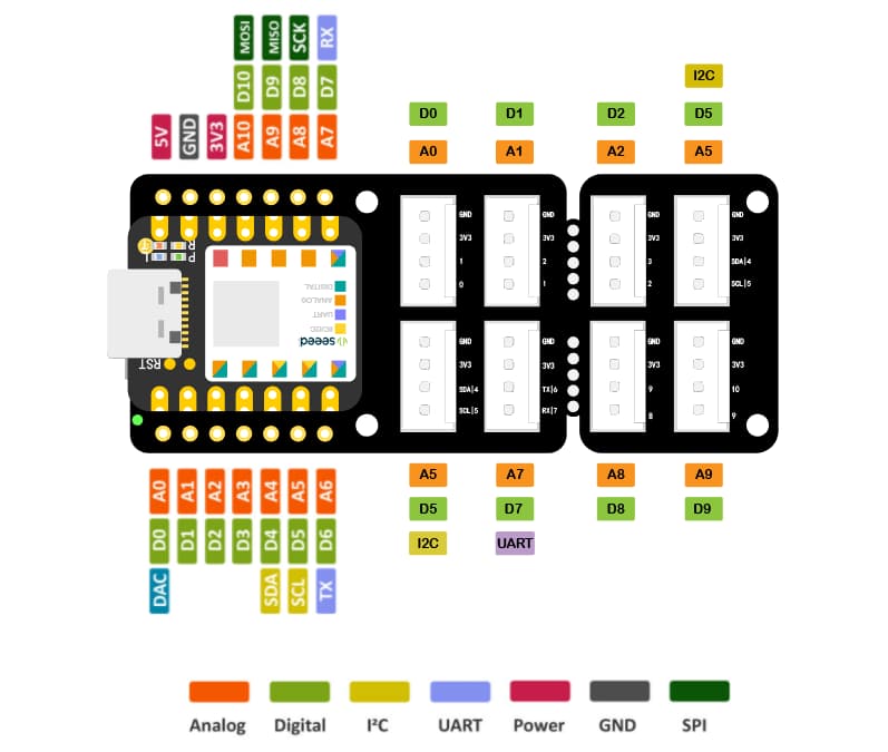
BTW , first in the rework would be a proper grove connector for the full SPI interface, (8,9,10) they try to keep the clock pin close (8) but suc’s when you trying to keep the wiring clean.
Yes Seeed Gove connectors have a multiplexing concept, by staggering the Data Pin a and b for a grove connector, it is possable, depending on coding to use 2 pins to give 4 connector options… it is not used as much as before… but a vey powerful system
By staggering the Data channels-a and -b between connectors it is possable to multiplex connectors… one channel is typically a timing channel and one is a data channel… by multiplexing, the periferal unit can detect if they are recieving a timing or data channel and they will ignore or accept as appropriate… This is the beuty and elegance of the system…