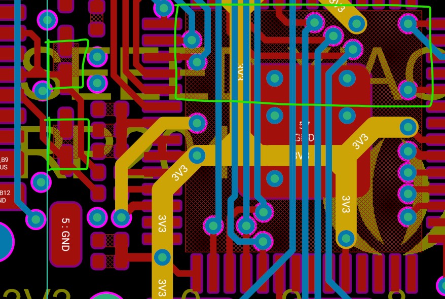
I was checking the PCB design of XIAO RP2040, noticed there are some cross hatched area on the top layer. As I’m a rookie and have no experience about Altium Designer, just wondering what are these.
Thanks.
I think those areas should be ground layer