On pcb if s2 is for ac/dc what is s4?
Sorry, what do you mean?
On the dso quad schematic you find on chB s4 cpc1017 if I am correct s2 is used for ac/dc input. What is s4 used as?
I can see it controles the opa just dont know why. Just Interested sorry if daft
The input signal is attenuated by the potential divider network formed by R2,R2A,R4,R4A,R6 and R6A. S4 is used to connect U2B to the input attenuator in the more sensitive ranges and disconnect it from the attenuator in the less sensitive ranges. The signal being measured is thus applied to later stages either by U2A or by U2B depending on the v/div setting. The outputs from U2a or U2B are further selected by U16. I hope this answers your query.
Yes, a big thank you
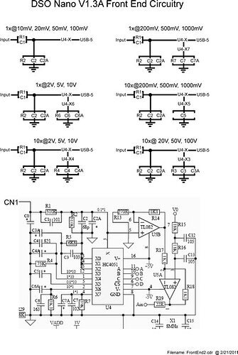
Would you be willing to construct a simplified front-end signal diagram for the Quad for each range setting? If you don’t have the time, I would do it if you help me to determine the gain components for each range.
I am also interested in that 10x probe compensation cap and how it interacts with everything.
The Nano attachment demonstrates what I am talking about for the Quad.
I had actually already thought of redrawing the analog circuit so that it shows the signal path more clearly. The original diagram is drawn in a confusing way making it appear more complex than it actually is. Unfortunately I am away for a fortnight but I will look at it when I get back and post the diagram here.
as for the CHA:
- S1: AC/DC selecting;
- how to select the range: actully, for the X1 probe: 50mv/div,100mv/div,200mv/div,500mv/div --U1B,select with U3_Y
1v/div;2v/div;5v/div;10v/div —U1A,select with U3_X
select the U1A/U1B with U5
3.S3: when there is a high voltage, there will be high voltage on the R3, without the S3 shuttign down the U1B, it will be possible for the high voltage damage or breakdown the U1B, so , the S3 was added to isolate the high voltage. so , a Optocoupler was added before the U1B but not before the U1A because U1A is designed to adop high voltage and has a high attenuation ratio.
