Hello Carmen,
Thank you for your fast response. I sent the e-mail dates and addresses in PM.
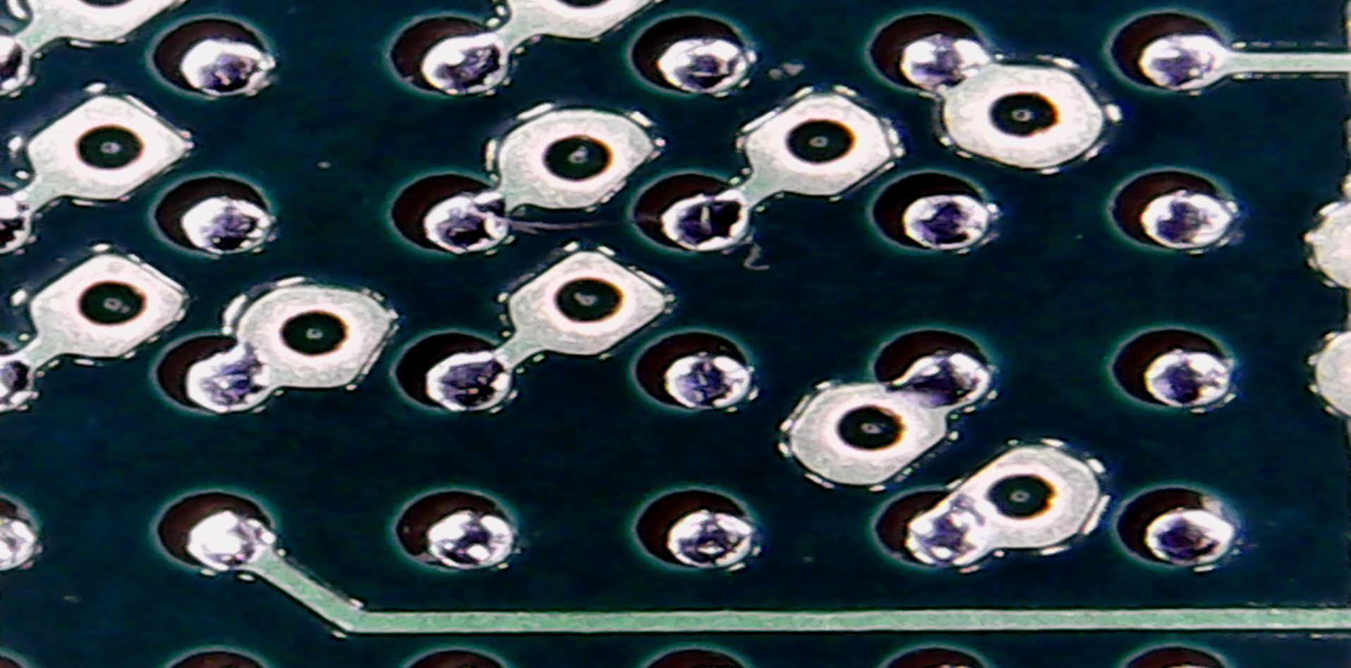
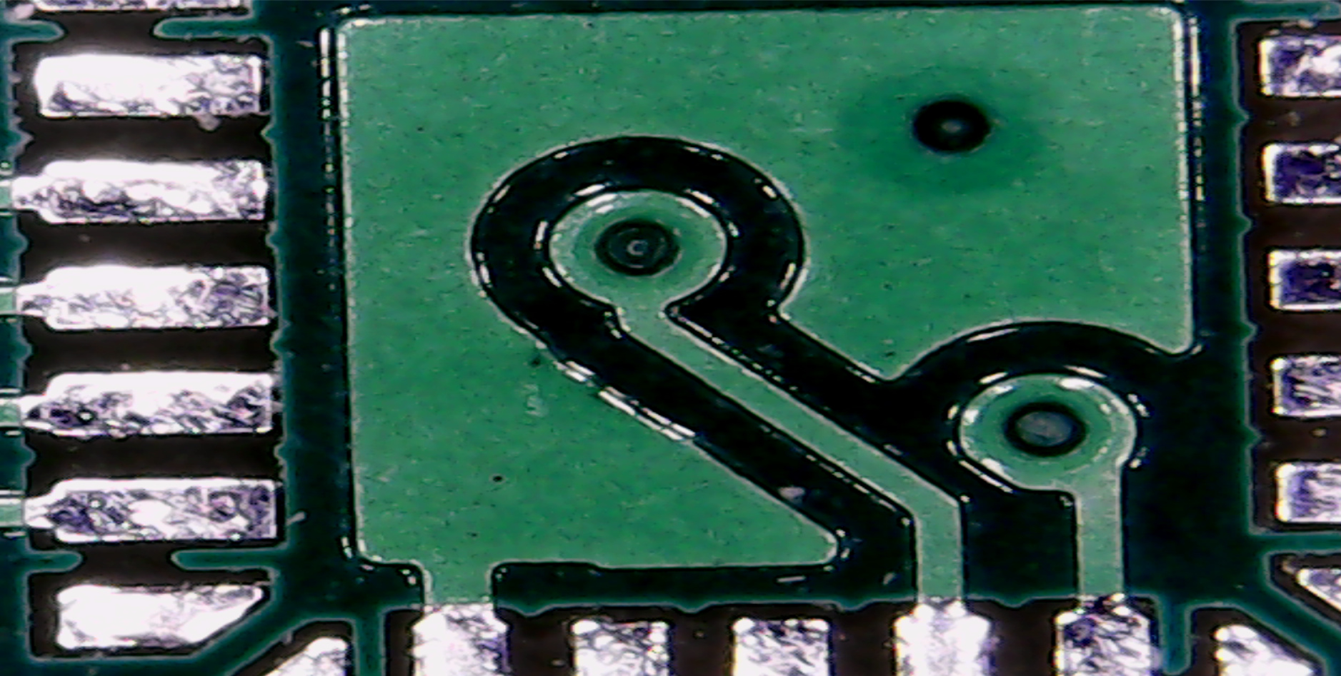
The clear photos of the PCB (BGA area) are attached. Also I attach a photo of different PCB (our design, two layers) that we got from Seeed at the same order. You can see the difference clearly.
I also check the vias with the multimeter, I can see the conductivity on vias. Because of the BGA pins are close to vias, they have to be masked.