Hi,
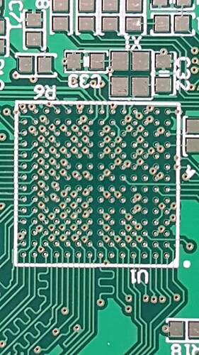
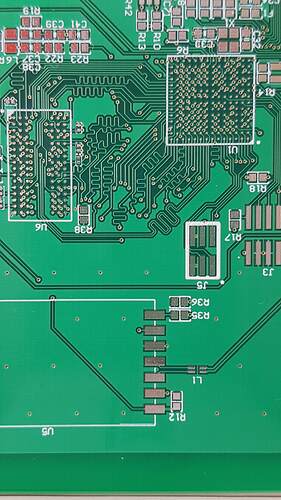
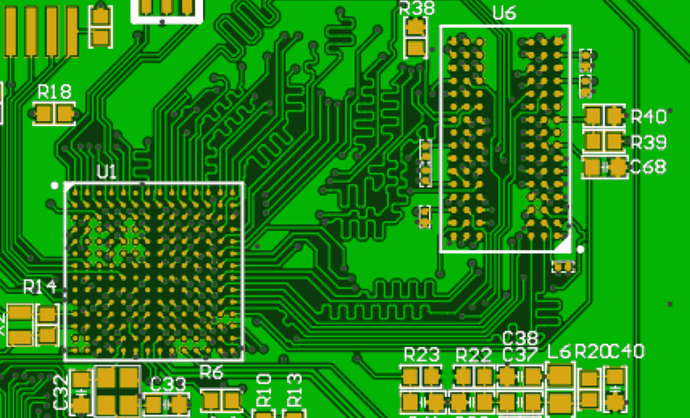
I have ordered 7 different Fusion PCB products (Order #181101191000). We have problem with one of the products which is 4 layered. The product wasn’t produced as we wanted. Although all the vias are tented in our design files, most of them are not been masked on manufactured PCBs. Solder mask quality is not good. Especially vias under the BGA ICs (fanout vias) have to be tented but all the fanout vias are naked. Because of this reason we CAN NOT SOLDER the BGA ICs.
I sent 3 e-mails since I got the PCBs (fusion support and manufacturing service) but there is no answer. I am still waiting a response.
Manufactured PCB photos and design views (EasyEda) are attached.
Hello Alpay,
Thank you for letting us know. I have checked our support system and it seems we haven’t received any e-mails from you to our general support since the 2nd of November, which was regarding another issue. Could you PM me the e-mail address you sent them to?
Also, regarding your problem with the PCBs, are you able to get a clearer picture? The reason for this is because the BGA pads that are supposed to be open appear silver in color. That is, they have been opened in the solder mask layer and you can see the HASL finish. The other vias in the BGA that are supposed to be tented appear the same as the other vias on the board, that is you can see the orange color of the copper coming through a bit. This suggests they are tented and shouldn’t affect soldering.
Hello Carmen,
Thank you for your fast response. I sent the e-mail dates and addresses in PM.
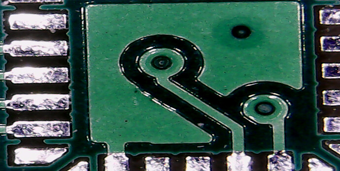
The clear photos of the PCB (BGA area) are attached. Also I attach a photo of different PCB (our design, two layers) that we got from Seeed at the same order. You can see the difference clearly.
I also check the vias with the multimeter, I can see the conductivity on vias. Because of the BGA pins are close to vias, they have to be masked.
Thank you Alpay, these photos are much clearer but they raise some other questions. The difference between the two photos is obvious but you can also see the edge of the BGA pad opening between the via and pad.
I have forwarded the case to the quality assurance engineers for a second opinion and they will get back to us soon with their verdict.
We won’t be long,
Hi Alpay,
Thank you for your patience, the quality assurance team have got back to me and they say that the vias are tented but the solder mask is just a little thin. This is within IPC-class 2 standards however and about 30% of boards will come out like this. For BGA via tenting, they suggest soldermask filling to ensure they are fully covered, otherwise smaller drill holes should help with the tenting.
On another note, I think if a paste/reflow method was used to solder the BGAs then the boards should still be workable. The stencil should only allow paste to be applied to the BGA pads and the soldermask dam still exists which would stop the solder from flowing into the holes.
Nonetheless I have given you a coupon for all the trouble but as mentioned before, we cannot guarantee that the boards will not come out the same in future orders.
I hope that is alright, and let me know how it goes,
Hi Carmen,
Thank you for your help.
This board is the first sample of our design. I will try to solder but if there will be an error we may not see the source of the problem (design or solder).
I will inform you when I try.
Thank you! And all the best!
