Preparing Gerber files from Eagle

Hi,

I’m new to creating Gerber files and have some questions.
I’m using Eagle to make a double sided board.

  1. Do I need to flip/mirror the bottom copper/silk/mask files when I run a CAM job in Eagle?
    (this is my biggest worry!)

  2. Do you have any naming conventions for each layer?
    for example…

    (please check http://www.ece101.com/2008/09/creating-gerber-files-in-eagle/ for full details)

3) Can you do slotted or exotic shape PCB like this example?
I attached image again - please check thanks

slotted_pcb.gif

  1. Can you do any board thickness between 0.8mm and 1.6mm - for example 1mm?

  2. Finally, do you have a DRC file for Eagle that we can download?

thankyou

Hi

Thanks your post. :slight_smile:

q1:Do not need mirror or flip the bottom layers to top.
q2:Here is out fileseeedstudio_cam.rar (980 Bytes)
q3:sorry,I can’t see the picture, would you attach it again? you meant the flash pads or drills?
q4:yes, the limit is 0.4mm~2.4mm, 1mm is OK.
q5:here it is :seeedstudio_rule.rar (970 Bytes).

Please let us know if any question or info needed. ^^

Thankyou very much for your helpful reply!

Each layer in the CAM file has the same name (‘Solder stop mask SOL’)- could you rename for beginners?
example:- Top_Silk/Top_Copper/Top_Mask/Milling/Holes etc…

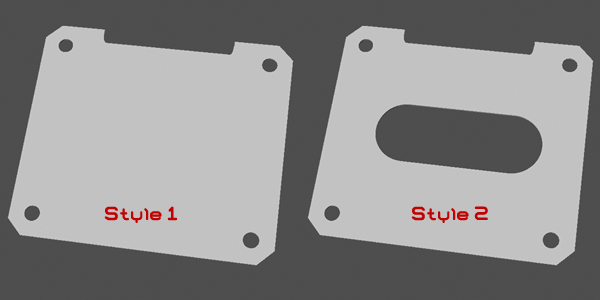
Sorry, I re-attached in my first post above - please check if we can do style 1 or style 2.
Also if you have any example of complex board shapes that you could show us that would be nice.

Thanks,I can see the picture now.
yes,we can make that.

The cam files are same name, but different postfix.
example:top silk–>xxxx.tsi ; top copper–>xxxx.tco …etc.(“xxxx” is the PCB’s name).

postfix ===== layer
.tsi ===== silk top
.bsi ===== silk bottom
.tco ===== top copper
.bco ===== bottom copper
.tso ===== mask top
.bso ===== mask bottom
.tpm ===== padmask top
.bpm ===== padmask bottom
.do ===== drilllegend & boardoutline

OR:seeedstudio_cam.rar (1001 Bytes)

Please let us know if any question or info needed. ^^