First of all sorry for my english. It’s not well but I hope you will understand me.
For some time I try to find out how does this configuration below work? I’d like to use it in my own hobby project because I assume it’s appropriate.
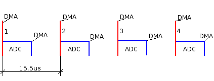
Please correct me if I’m wrong - I discovered that period od generated events is (PSC+1)*(ARR+1)/72MHz.(am I right?)
What is the meaninng of bits UDE and TDE when DMA is invoked by end of ADC1 convertion? What is the conception of this configuration?
I took small experiment with this configuration with set bits UDE and TDE and without them but I can’t notice any difference in gathered data in memory. I believe it has deeper sense.
I would be very very grateful if you could help me.
[code]TIM1->PSC = 30;
TIM1->ARR = 35;
TIM1->CCR1 = (35+1)/2;
TIM1->CR1 = 0x0094;/0000 0000 1001 0100
|||| |||| |||| |||±–CEN=0
|||| |||| |||| ||±—UDIS=0
|||| |||| |||| |±----URS=1
|||| |||| |||| ±-----OPM=0
|||| |||| |||±-------DIR=1
|||| |||| |+±--------CMS=00
|||| |||| ±----------ARPE=1
|||| ||+±------------CKD=00
+++±+±--------------Reserved/
TIM1->RCR = 0x0000;/0000 0000 0000 0001 Repetition counter register
|||| |||| ++++ +++±–Repetition Counter Value=1
+++±+++±------------Reserved/
TIM1->CCER =0x0001;/0000 0000 0000 0001
|||| |||| |||| |||±–CC1E=1
|||| |||| |||| ||±—CC1P=0
|||| |||| |||| |±----CC1NE=0
|||| |||| |||| ±-----CC1NP=0
+++±+++±+++±-------Reset value/
TIM1->CCMR1=0x0078;/0000 0000 0111 1100
|||| |||| |||| ||+±–CC1S=00
|||| |||| |||| |±----OC1FE=1
|||| |||| |||| ±-----OC1PE=1
|||| |||| |++±-------0C1M=111
|||| |||| ±----------OC1CE=0
+++±+++±------------Reset value/
TIM1->BDTR =0x8000;/1000 0000 0000 0000
|++±+++±+++±+++±–Reset value
±--------------------MOE=0/
TIM1->DIER =0x4200;/0100 0011 0000 0000 DMA/Interrupt enable register
| || ±—CC1IE=0
| |±------------UDE=1
| ±-------------CC1DE=1
±-------------------TDE=1/
TIM1->CR1 |=0x0001;//CEN=1, TIMER1 Enable[/code]
This is my vision of this configuration: