Hi Shazam & DwaineR,
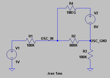
below is the schematic of a worst case scenario for DC offsets. V1, R1, R2 & R3 conforms a resistive divider. R4 & V2 model the RV2 DSO input (in the figure V2 is set to 0 → connected to GND).
Let’s assume that DSO is not USB connected (otherwise R3 will be probably shortcircuited).
First case → No DSO attached (ideal value)
OSC_IN = 900 mV
OSC_GND = 100 mV
OSC_IN - OSC_OUT = 800 mV
Second case → R4 tied to OSC_GND (V2 = 0)
OSC_IN = 844 mV
OSC_GND = 155 mV
OSC_IN - OSC_OUT = 689 mV
Third case → R4 tied to OSC_GND + Offset (V2 = 1.5V)
OSC_IN = 948 mV
OSC_GND = 51 mV
OSC_IN - OSC_OUT = 896 mV
Fourth case → R4 tied to OSC_GND + Offset (V2 = -1.5). Equivalent to reverse connections in DSO
OSC_IN = 741 mV
OSC_GND = 258 mV
OSC_IN - OSC_OUT = 482 mV
Two conclusions are clear to me:
-every circuit you can design modifies circuit under test
-if VREF is non zero in the RV2 circuit, there is an offset which depends of the circuit under test. In the case presented was 200 mV depending of the form of measurement. If resistors were smaller (say 100K) offset accounts for a small 20 mV which is perfectly reasonable. But even if VREF is zero, there is some error (in this case the orientation of the DSO has no importance)
BUT (and that’s a big one):
-Are you usually work with MOhm circuits with a 1MOhm input? → This is absolutely crazy IMHO
-Is it better to have a variable input impedance to work with (each scale a different measurement)?
As mentioned before, the circuit has it’s drawbacks.
Discrete variable input gain can be simply and easily done with solid state relays (like ASSR-1218 - 0.8€ @ 100 - mouser). The problem associated to them is size. But maybe is an option to consider. If VREF has to be 0, then bipolar power supplies are needed and the first circuit i posted can be used with minor modifications.
Side note: i think the purpose of redesigning a stage is to enhance it. Original DSO has DC coupling and 80 Vpp (selected to fit display range) for a x1 probe. Obviously you can modify some of the design constraints but i think you can’t redefine them all.
Slimfish
Edit: i forgot the schematic!!!