sorry if i bothered you with the circuit explanation of my last message. My intention was not to teach you but to show other people how the proposed circuit works. i’d like to emphasize that this series of posts are not because of my ego. I only want to contribute to enhance a product which can be very useful in my day work (when enhanced) and for many other people (like electronic enthusiasts).
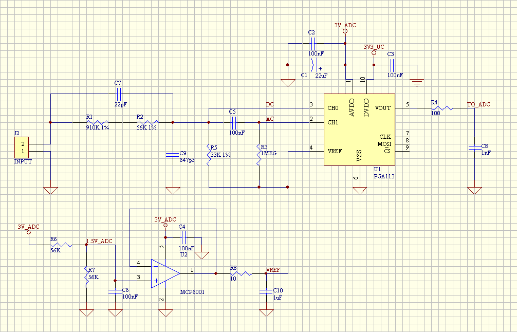
The last circuit i posted had another error. This time was due to the drawing hurry (was done in 15 min). R5 and R? (i forgot to name it) are not grounded but connected to VREF. This is important, otherwise input can not cope with negative values.
Suppose the ADC can resolve 10 bit maximum with a VREF of 3V. That’s 2.9 mV/LSB. If offsets are in the range of 100uV, and we use a gain of 100 for the 10 mV/div, then we have a 10 mV offset which can be resolved by the ADC.
They cost thousands of bucks not only because the DC/AC resolution, but because of the sampling speed. And of course, for the functions they offer.
Both presented circuits cope with AC and DC coupling for the full range of inputs. And i think they are not complicated at all (even easier to adjust). And as showed, you need no split(±) supplies, otherwise, the PGA113 would not fit the bill (5.5V max).
If you get a 100kOhm resistor and use a 900kOhm in order to have a 1Mohm input then you have a resistive divider with a gain of 9/10. That’s fine when you have a signal with an amplitude smaller than 10/9 of VCC, which is not the case of DSO Nano, capable of -+40V with a x1 probe.
Again, in order to have a ±40V input with a x1 probe it’s necessary to atenuate the signal first. If you connect a x10 probe to the input, then signals will be very small and they have to be amplified (every mV is important).
There is no need to have a variable offset input when you can select between AC or DC coupling. The original scope doesn’t have a real AC coupling and the offset “simulates” and AC coupling by adjusting with the PWM the DC component. The PGA113 amplifies the signal in relation with VREF making the AC “simulation” a challenge programming effort in the case of this PGA.
You’re right, for two channel, up to 300 ksps are possible. But samples are not taken at the same time, so the aliasing probability is very high.
Thank you but no. What i need is a self contained oscilloscope for field use. And it’s not complicated to have an oscilloscope which enter low power mode if battery gets depleted (PGA113 has a software shutdown mode).
SCHEMATIC from Slimfish of 6-22-2010
A few changes suggested:
• AC Couple both channels.
• Delete the 1 MOhm from IC pin 2. This also allows using a 1 nF or 0.1 nF COG (do not use X7R, X5R, Y5U, etc.) on pin2. → You’re right with the previous schematic. But this resistor is not connected to GND (see new schematic) and thus is needed anyway.
• R1, R2, C7 need to be 805 or 1206 for >200V capability. C7 and C? (647pF to GND) need to be COG types
• Delete C8, the ADC has enough capacitance. If a low pass filter is desired here, increase the value of the 100 Ohm resistor and use the input capacitance of the ADC to calculate R. → The ADC input capacitance is about 5 pF. It’s very dangerous to count on such small (and variable) values to conform a low pass filter. But as showed on current DSO Nano it works…
• Delete the entire Vref section (OpAmp and related parts). Connect pin 4 of the PGA113 to the same place as U5A pin 3 (R13 - C16 junction) in the current DSONANO. → No, you cant. VREF is a low impedance one (3.25 kOhm -see datasheet-) and hence the PWM filter will not function as intended.