Just got my DSO203 from SAIN. It has HW version 2.72, SYS 1.60, App (PLUS A1) 1.10.
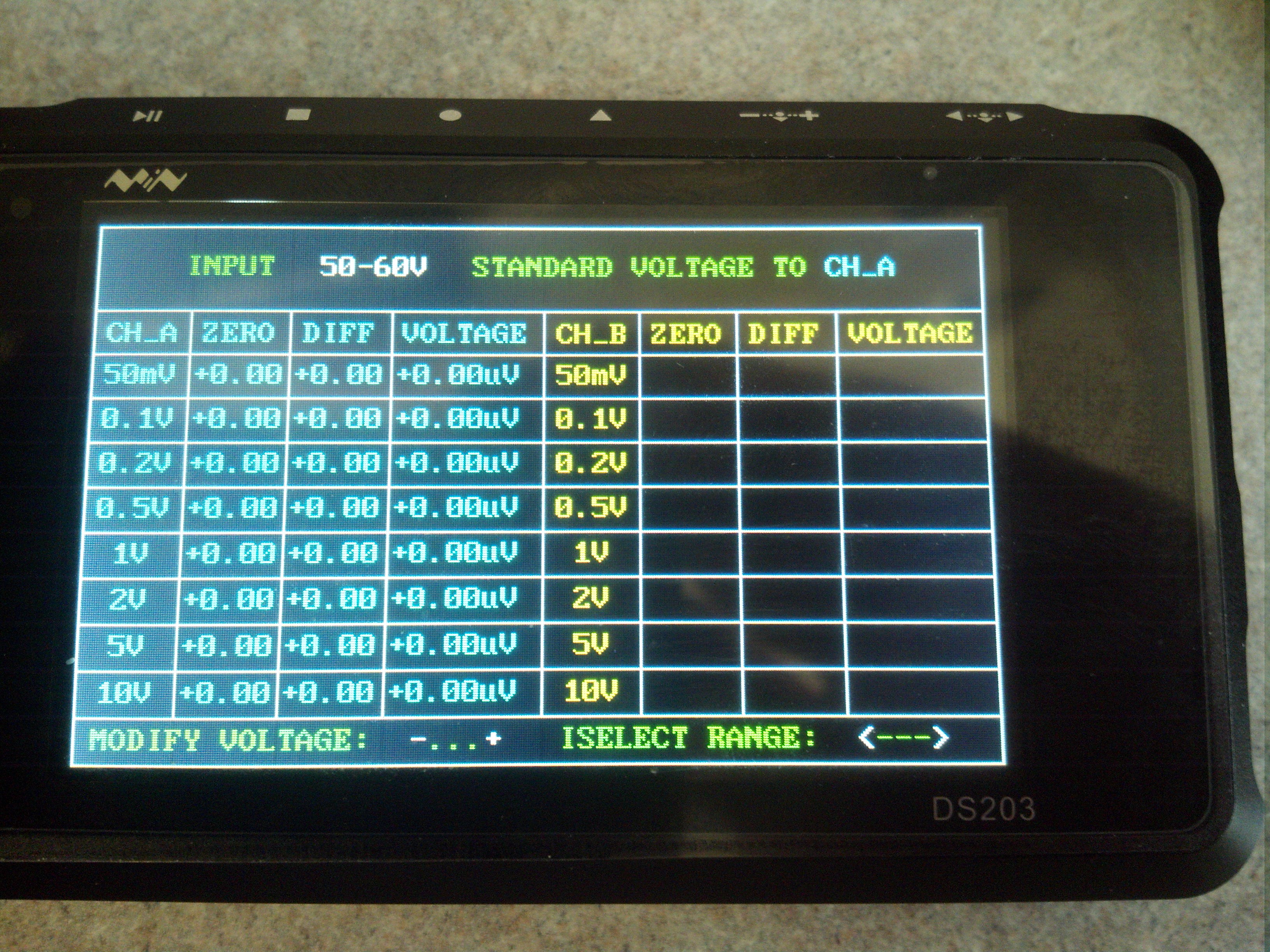
I decided to calibrate it. Started with CH A.
Followed the directions given on the screen:
.250mv
.5V
…
11-12V
At this point I was still good, adjusting a few % here and there.
Then I got to :
50-60V
I set the voltage gen to 55. At this point, the probe got hot. I disconnected it.
Now, the CH A is short, it measures 170ohm. (And obviously doesn’t measure anything).
CH B and Wave Out still work.
I am able to solder surface mount components, if you guys can point me to which component needs to be changed.
Also, I need to know how to remove the metal shield (or if I need to remove the metal shield to get to the circuit).
Did I do something wrong during the calibration ? I know it says not to exceeded 80V pp, and I was way bellow that.
I’m surprised the probe got warm. In x1 mode it is a straight connection through from tip to connector so there is not really anything to dissipate any power in the probe.
When you say you measure 170 Ohm, where are you measuring that? Straight at the DSO socket or via the probe? Are you sure there is nothing wrong with the probe?
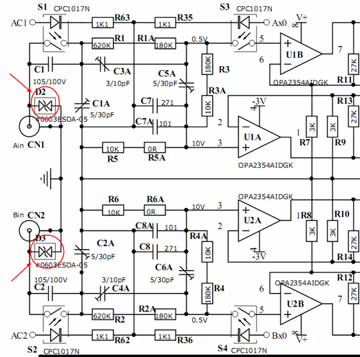
I have a 2.70 schematic but not a 2.72. I’d guess the i/p circuitry is similar or the same. The input point is connected to 800K resistance (680K + 120K in series) before it goes anywhere else. There is an AC coupling capacitor rated at 100V but even if that shorted it would just mean the AC coupling didn’t work. There is also an opto solid state relay to bypass the AC connection but that is rated for 1500V isolation so fairly unlikely to blow.
So nothing obvious to display this symptom and a bit of a puzzle unless there is some short on the PCB causing a problem.
Personally, I would be returning it as a faulty item. If you did want to pursue it further then you do have to remove the metal shield by unsoldering it. I have done some work just by unsoldering it at one end and lifting it up a bit to get access to the parts I needed.
The probe was warm for sure, at the base where probe plastic ends and wire begins. I guess since I had a serious power supply.
The 170ohms resistance was measured across the port CH A, with or without the probe. Probe by itself was not shorted.
CH B is in mega ohms (or open).
I also thought that I should return it as a faulty item, and I sent e-mail to SainSmart.
They replied with this :
They attached (and I attached here) the schematic snippet with the location of the D2 and D3.
Strange that they would ship this if they knew it was a problem.
I’ll try to remove those parts, since I can get someone at work to do it.
About the shield: It seems difficult to pull out the shield/circuit board/buttons/connectors assembly. Do I need to pull a certain way ?
Those 2 diodes are not present on 2.6 and 2.7 hardware so must be a recent addition to 2.72. Seems like a stupid idea to me as the series resistance gives the major protection here and those seem to be rated at 35V clamping voltage… If they were going to fit this type of thing then should berated at more than the normal i/p of the scope which I believe is 80V.
If you wanted to push it they seem to be saying that it is a problem and these devices will be removed on future shipments. That should give you grounds to get it replaced.
If you want to proceed with removal I just desoldered about 4 of the solder tabs on teh shield and bent it up. Of course, it is possible that the shield has also changed with 2.72. Maybe post a picture if you can.
There were 3 place to desolder the shield, and it came off completely.
Then I gave it to our work guy who has the serious double iron for just this kind of stuff. He quickly popped D2 and D3 off.
That fixed channel A, it now works correctly.
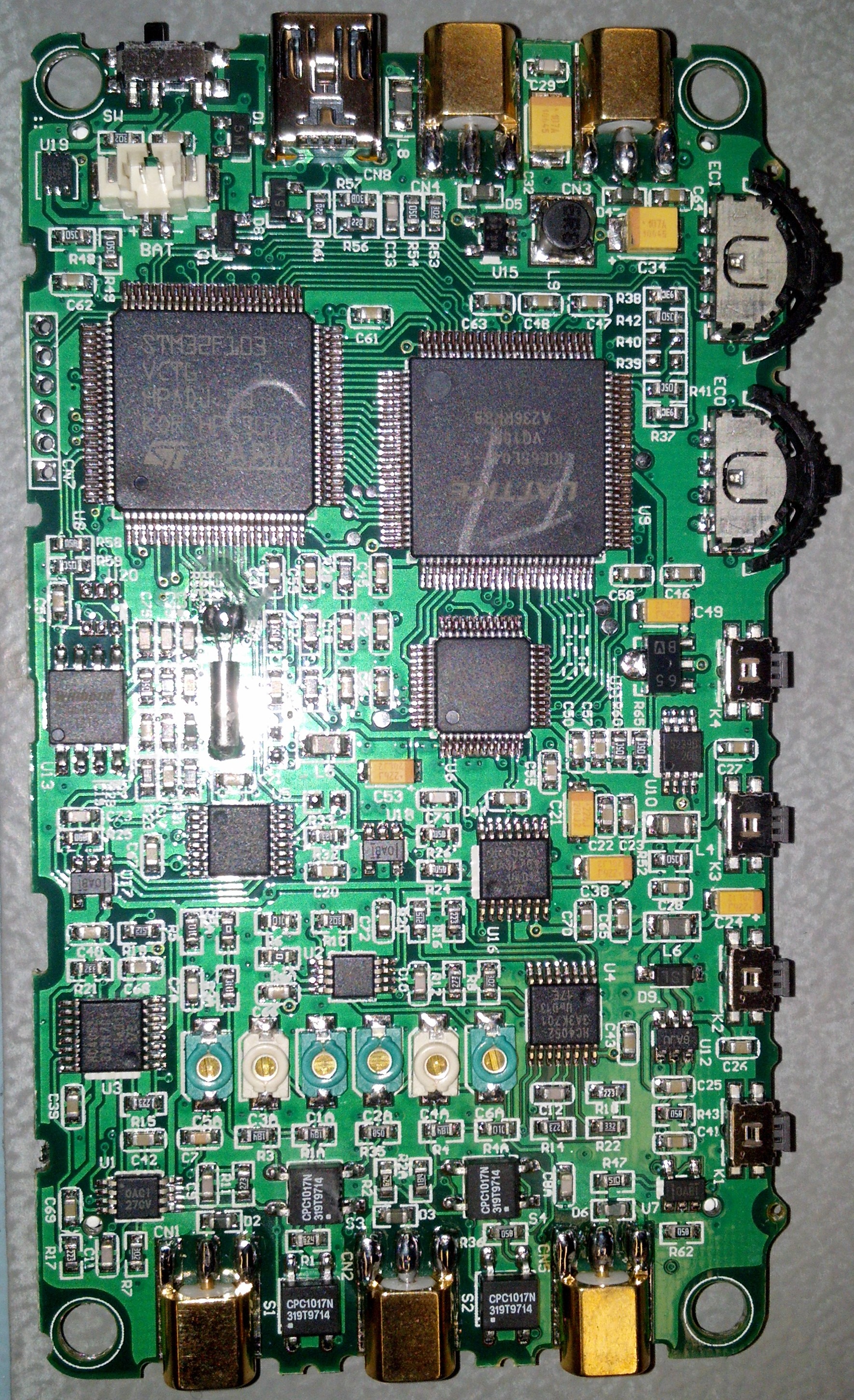
I am attaching a crappy cell phone picture of what’s under the shield for this 2.72 HW.
This is a before shot : you can see D2 and D3 clearly marked closer to the bottom.
Good to hear you fixed it. This is obviously a hazard on new 2.72 boards until they remove those components on the analogue inputs.
It was interesting to see the picture because it also shows the digital inputs at the top. Here one can see that they have replaced the previous D5 ESD covering both the inputs with two separate diodes probably of the same type as on the analogue channels. That is good news because previously the type of diode used and its positioning after a 11K resistor meant that the performance of the digital channels was severely degraded unless one hacked this. The threshold of the new diode should not be a problem for normal use of the digital channels and now the digital channels should work OK by default.