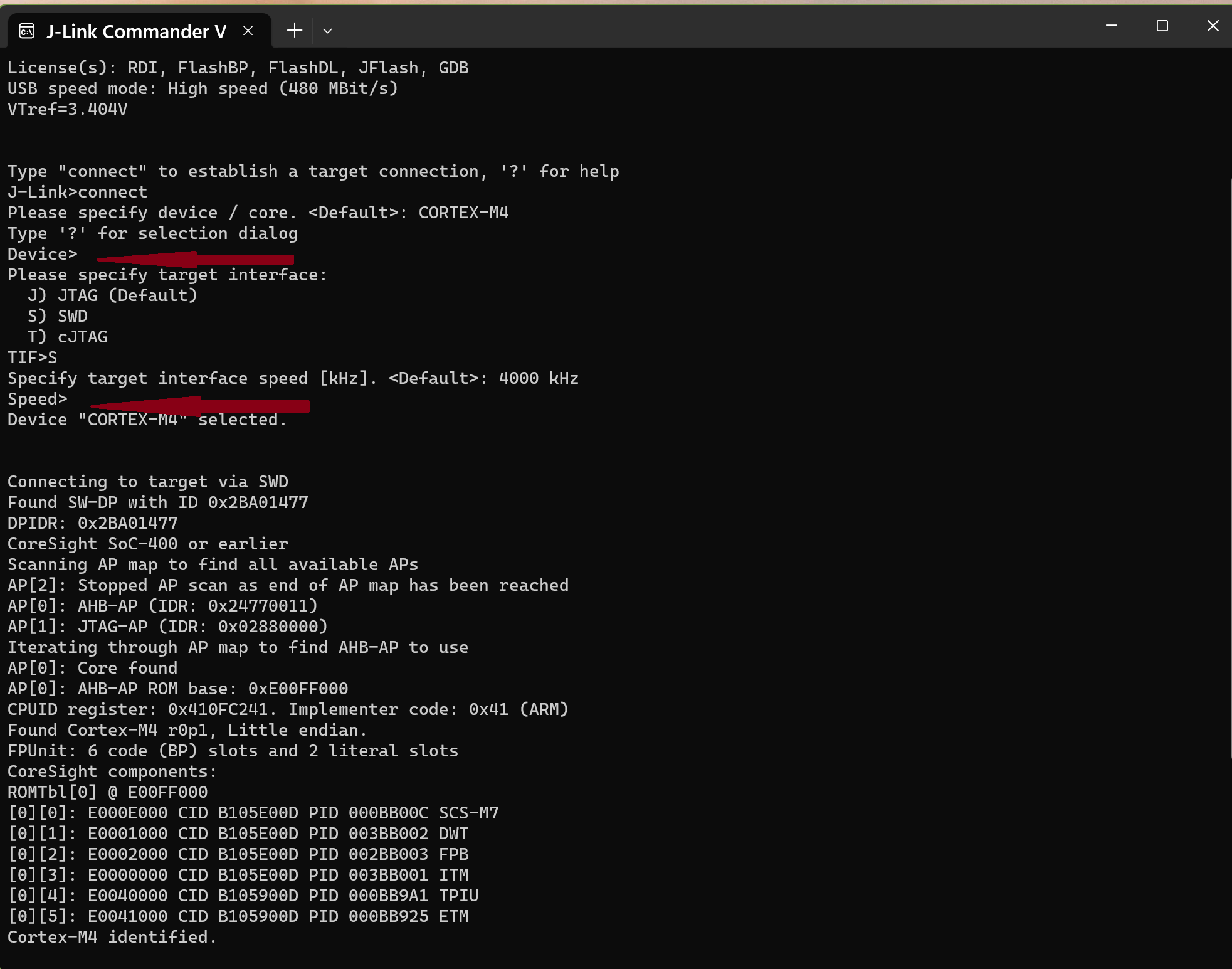
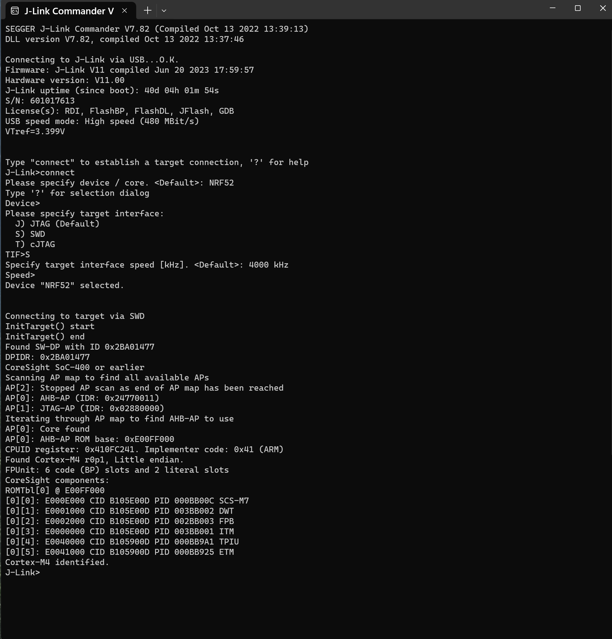
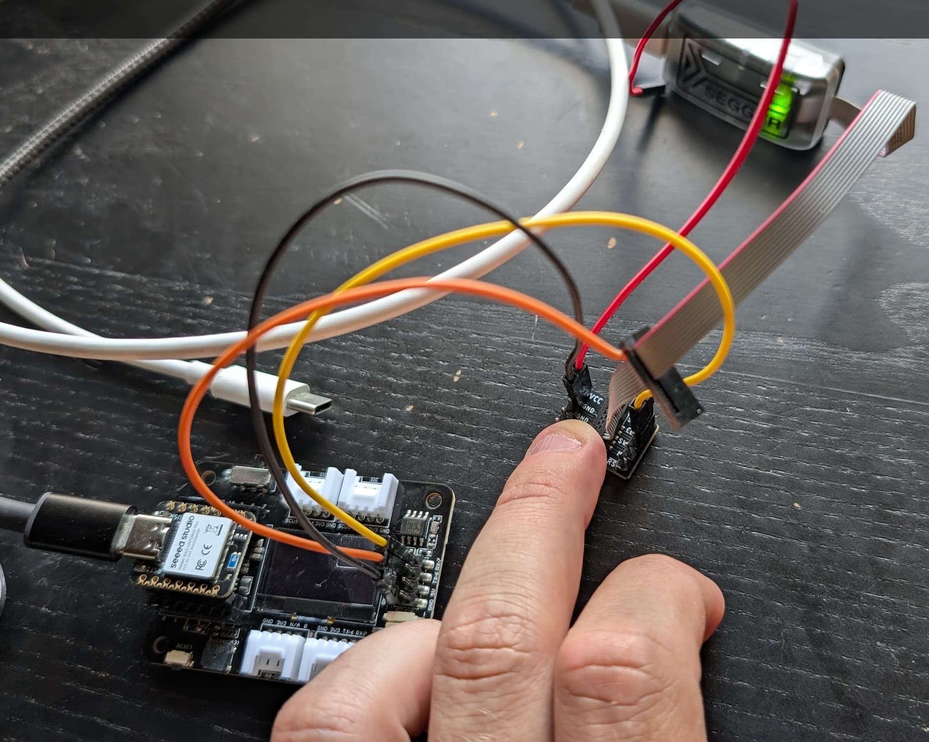
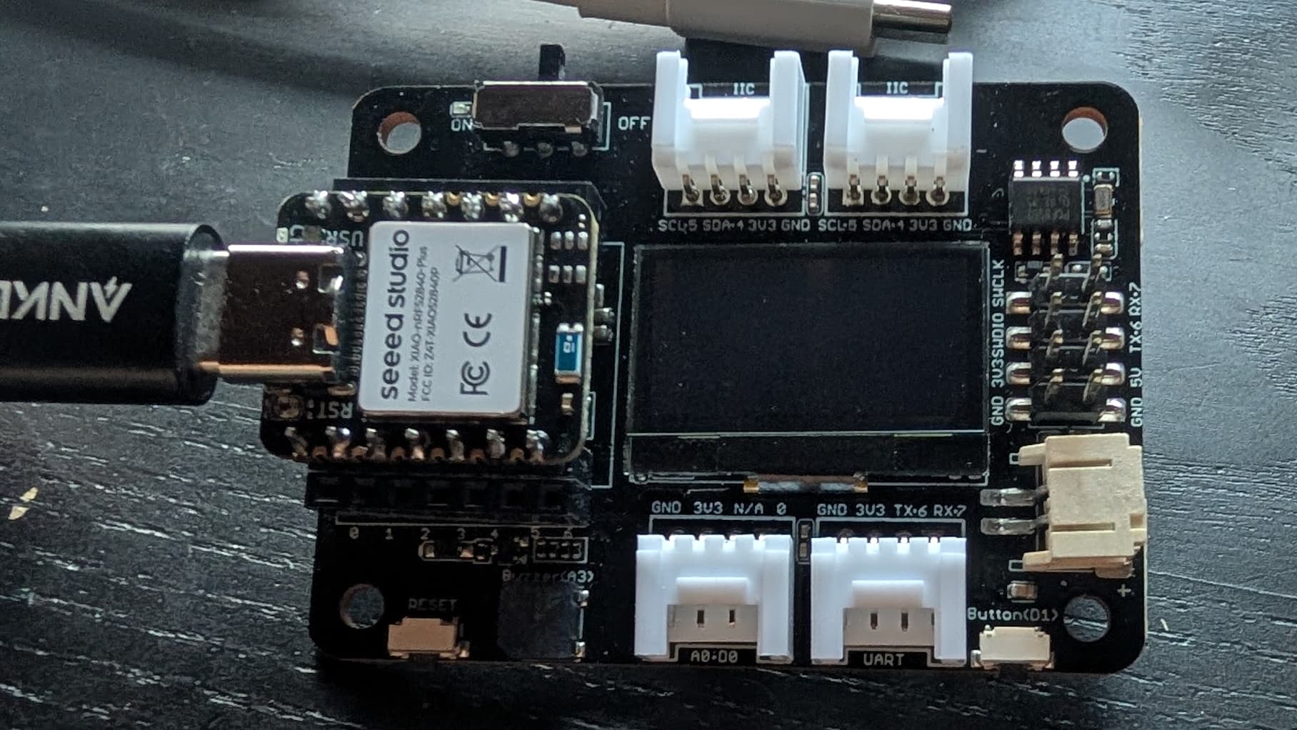
Here is my AI summery Document, Thank you sir!
# J-Link SWD Debug Session Report — XIAO nRF52840 (Sense)
**Date:** 2026-09-09/10 (CST)
**Probe:** SEGGER J-Link V9 (HW V9.70, FW compiled 2021-05-07), S/N 20781318
**Target:** Seeed XIAO nRF52840 (Sense), combo firmware (S140 SoftDevice @ 0x0 + Adafruit UF2 bootloader @ top of flash)
**Host:** macOS (J-Link SWD software V9.34b installed via cask)
**Goal:** Verify whether the J-Link probe can connect to the nRF52840 over SWD.
—
## 1. Executive Summary
**The J-Link probe, host software, cabling, and target power are all verified healthy. The target’s SWD debug port does not respond at the physical (DP) layer — no ACK is ever returned for the DP IDCODE read, across four independent software stacks and four clock speeds. All software-side causes are ruled out. The failure is electrical: the chip either has its debug port locked (APPROTECT) or its SWD front-end / the board’s SWD path is defective. The two remaining discriminators are a known-good target board and/or a known-good probe.**
—
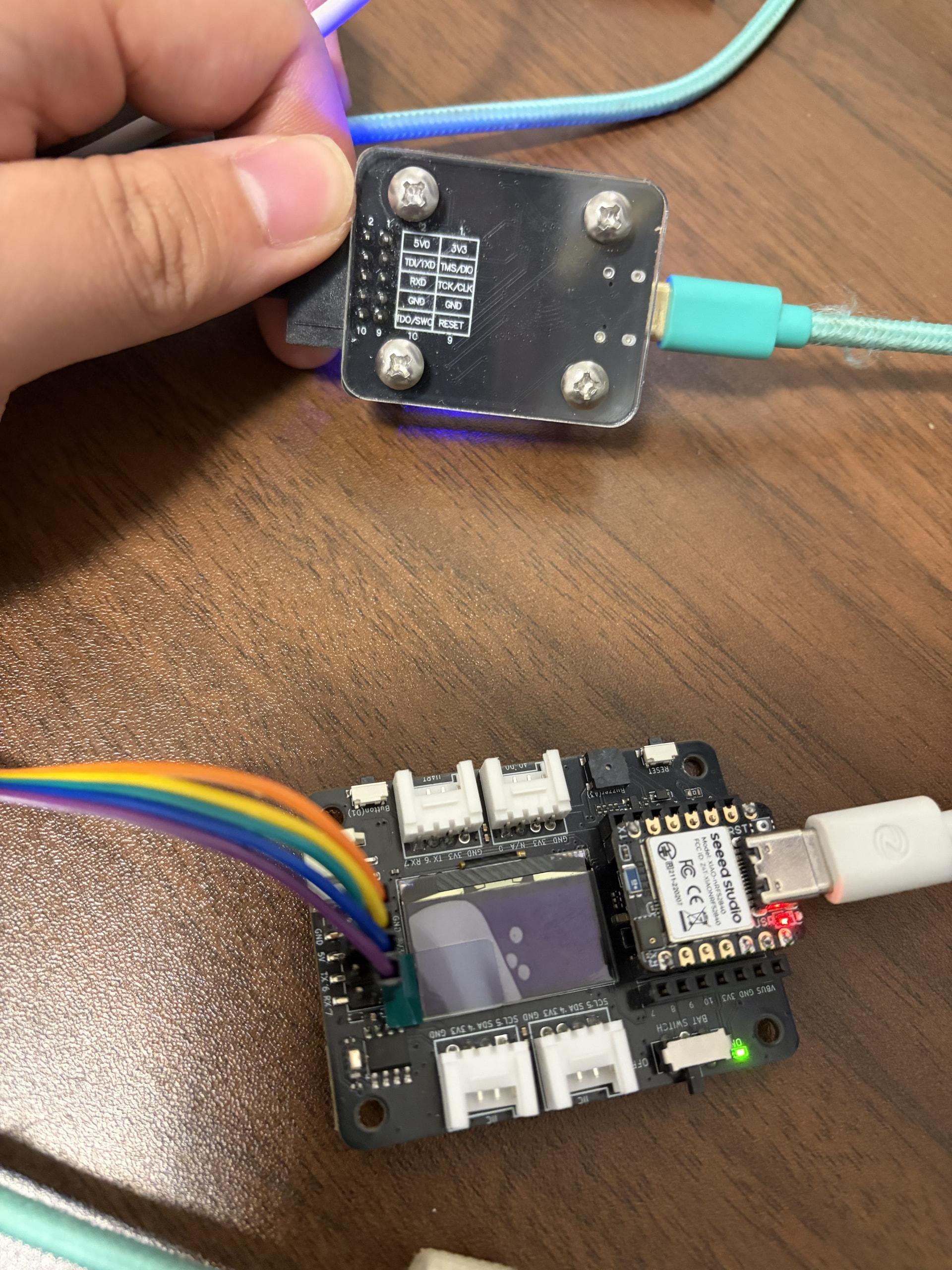
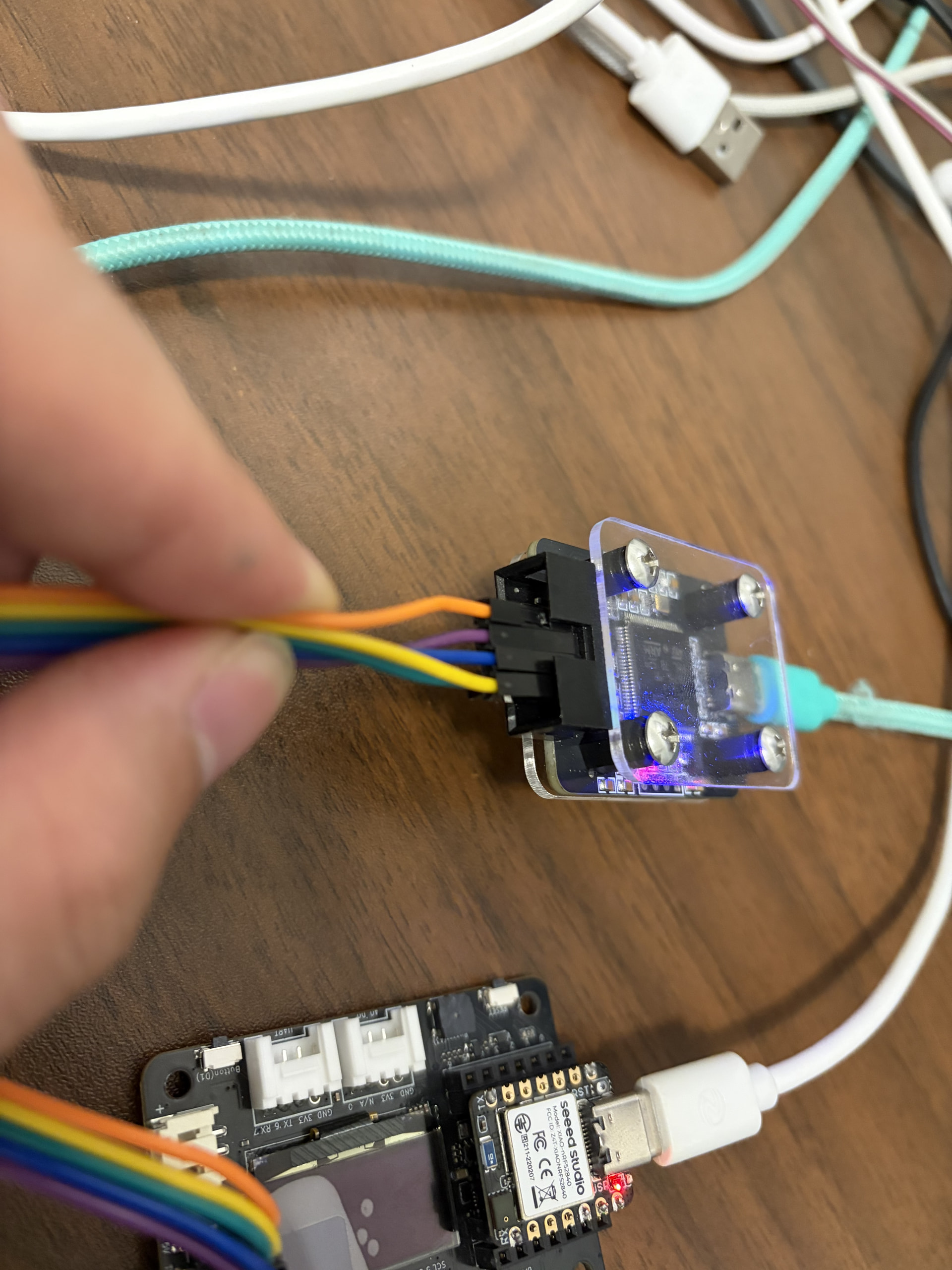
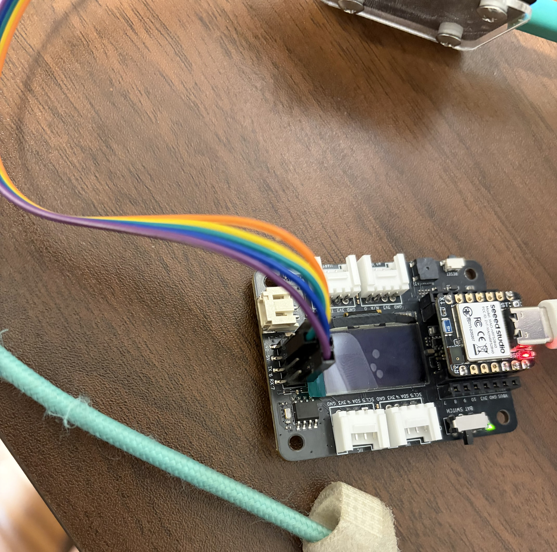
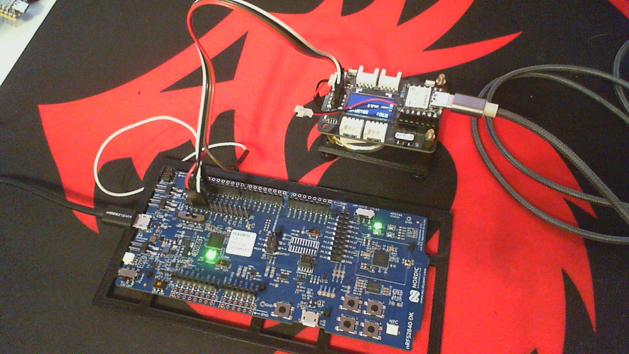
## 2. Hardware Setup
| Item | Detail |
|—|—|
| Probe | SEGGER J-Link V9, HW V9.70, FW 2021-05-07, S/N 20781318 |
| Probe connector | 9-pin SWD (1=VTref, 2=SWDIO, 3=GND, 4=SWCLK, 9=nRESET) |
| Target wiring | XIAO SWDIO → J-Link TMS/DIO; XIAO SWCLK → J-Link TCK/CLK |
| Ground | Common ground wired between probe and board |
| Target power | USB from host (3.3 V rail sensed: VTref = 3.25–3.27 V) |
| nRESET | Initially **not connected**; connected later (J-Link reports it cannot drive it low — see §5) |
| Board history | This XIAO has **never** been connected via SWD; all previous flashing was USB DFU / UF2 drag-drop |
—
## 3. Software Stacks Used (all independent)
1. **SEGGER J-Link Commander** (`JLinkExe` V9.34b) — proprietary SEGGER DLL
2. **probe-rs** 0.32 (CLI `probe-rs info`) — open-source, own J-Link protocol implementation
3. **Nordic nrfjprog** 9.4.0 (from Seeeduino Arduino package) — Nordic DLL
4. **nRF Connect for Desktop** (Programmer app, nrfutil stack) — Nordic’s current toolchain
5. (Attempted) Nordic nrfjprog 9.4.0 + **SEGGER libjlinkarm V9.34.2 dylib** via `–jdll`
—
## 4. Test Results Timeline
### 4.1 J-Link / probe identification
- macOS USB enumeration: probe found by both `probe-rs list` and SEGGER software.
- `nrfjprog --ids` → `20781318`. **Probe itself is fully functional.**
### 4.2 SWD connect attempts — JLinkExe
Script used (`swd_test.jlink`):
```
si SWD
speed 400
device nRF52840_xxAA
connect
exit
```
Result (identical at 100 kHz, 400 kHz, 1 MHz, 4 MHz):
```
Connecting to J-Link via USB…O.K.
VTref=3.267V
Selecting SWD as current target interface.
Device “NRF52840_XXAA” selected.
Connecting to target via SWD
InitTarget() start
InitTarget() end - Took 110ms
InitTarget() start
InitTarget() end - Took 111ms
Error occurred: Could not connect to the target device.
```
- No `Found SWD-DP with ID 0x2BA01477` line ever appears → **DP IDCODE never read successfully**.
- Generic `Cortex-M4` device also fails identically (rules out device-description issues).
### 4.3 probe-rs verbose (RUST_LOG=debug)
```
Performing SWD line reset
Reading DPIDR to enable SWD interface
Transfer 1/1 failed: Failed(NoAcknowledge)
```
Repeated ~10×. → The probe issues the SWD line reset and DPIDR read correctly; **the target never pulls SWDIO low to ACK** — no response at the very bottom of the SWD protocol.
### 4.4 Nordic nrfjprog
```
nrfjprog --memrd 0x10000000 --n 8
ERROR: Cannot connect to any nRF device.
```
Same failure as above.
### 4.5 nRF Connect for Desktop (Programmer)
```
Reading readback protection status for Application core
Failed … Device error: Setting the debug port SELECT register failed while
powering up sys and debug regions (Unknown error in the J-Link DLL (error code =-1)).
This might indicate that the debug port is unavailable. Double-check device
power supply and SWD lines, and ensure that SWD is not disabled
```
Note: the tool cannot even complete the debug-domain power-up handshake — consistent with a debug port that is either unpowered/unresponsive at the DP level or actively refused.
### 4.6 Recover / Erase attempts
```
nrfjprog --recover --family NRF52 --snr 20781318
Recovering device. This operation might take 30s.
ERROR: Recover failed.
```
- Also retried with the latest SEGGER dylib (`–jdll /Applications/SEGGER/JLink_V934b/libjlinkarm.dylib`) — same failure.
- nRF Connect “Erase all” also fails at the same step (protection-status read / debug-power-up).
- **Interpretation:** recover still requires an initial SWD DP connection (CTRL-AP is reached *through* the DP). Since the DP never ACKs, recover cannot proceed. Recover failure therefore does **not** prove APPROTECT — it only confirms the DP layer is unreachable.
—
## 5. Multimeter / Electrical Verification
All measurements taken with the target powered from USB.
| Measurement | Result | Meaning |
|—|—|—|
| VTref (J-Link senses target 3.3 V) | 3.25–3.27 V | Target power rail present; power wiring OK |
| Continuity J-Link pin ↔ XIAO pad (each line) | ~3 Ω, stable | Cables/solder joints electrically continuous |
| Wire-swap test (SWDIO/SWCLK swapped) | Still no connect | Not a swapped-wire issue |
| Re-soldering the connections | Still no connect | Not a cold-joint issue |
| SWDIO pad ↔ GND (**J-Link disconnected**, powered) | ~3 V | Chip internal pull-up active → pad truly reaches the chip’s SWDIO pin |
| SWCLK pad ↔ GND (**J-Link disconnected**, powered) | ~0 V | Chip internal pull-down active → pad truly reaches the chip’s SWCLK pin |
| SWCLK pad during connect attempt | **Voltage toggling** | J-Link clock signal does arrive at the pad |
| SWDIO pad during connect attempt | Only 3.3 → 3.1 V micro-dither | NOT a real 0–3.3 V data swing — looks like crosstalk, not an ACK |
| nRESET (after connecting pin 9 → RST) | J-Link warning: `RESET (pin 15) high, but should be low` | J-Link cannot pull the reset line low — nRESET does not reach the chip’s reset network either |
**Key conclusions from electrical tests:**
- SWDIO/SWCLK pads are the genuine debug pins (internal pull-up/pull-down states match nRF52 default debug-port behavior) and are connected to a live chip.
- The chip is alive: it enumerates on USB (visible as a second device in nRF Connect) — so the MCU core runs, ruling out System OFF / dead chip as the cause of zero SWD response.
- Clock reaches the pad, yet the chip never ACKs → the debug port is refusing or unable to respond.
—
## 6. Ruled Out vs. Remaining Hypotheses
### Ruled out (evidence-backed)
| Hypothesis | Why ruled out |
|—|—|
| Probe broken / not enumerated | Probe listed by SEGGER, probe-rs, nrfjprog; FW up to date (Configurator) |
| Host driver / software bug | 4 independent stacks, 3 different vendors, identical failure |
| Clock speed | 100 kHz–4 MHz all fail identically |
| Target not powered | VTref 3.27 V; USB enumeration works; SWDIO internal pull-up alive |
| Missing / wrong ground | GND wired; stable VTref reading |
| Swapped SWDIO/SWCLK | Swap test failed identically |
| Cold solder joints / broken wires | ~3 Ω continuity; re-soldering changed nothing |
| Pads not connected to chip | SWDIO=3 V (pull-up), SWCLK=0 V (pull-down) prove chip-side connection |
| Firmware re-purposing SWD pins | nRF52840 SWDIO/SWCLK are dedicated debug pins (QFN48 pin 26/27), not GPIO-muxed — firmware cannot steal them |
| Chip in System OFF / deep sleep | USB enumerates — core is running |
| J-Link firmware outdated | Configurator: “firmware already up to date” |
### Remaining hypotheses
1. **APPROTECT (read-back protection) enabled** — would explain a silent debug port; but the “IDCODE not even readable” symptom is atypical (APPROTECT usually still permits DP IDCODE reads), so this is **not confirmed**.
2. **Defective SWD front-end on the chip** (silicon or internal bond issue) while the rest of the chip runs fine.
3. **Board-level fault between the labelled pads and the chip’s actual SWD pins** that still passes static pull-up/pull-down checks but fails under driven signals (less likely given the pad measurements).
4. **Defective SWD output stage on the probe** (VTref sensing works, but the SWDIO/SWCLK line drivers may be dead) — cannot be confirmed without a second target.
—
## 7. Remaining Discriminating Tests (next steps)
1. **Known-good target board** — connect this J-Link to a second XIAO (or any SWD-capable Cortex-M board):
- Connects → J-Link is fine; this specific XIAO has a locked/defective debug port → treat as SWD-dead, keep using USB DFU, or replace board.
- Also fails → the J-Link’s SWD line drivers are defective → replace/repair the probe.
2. **Known-good probe** — if a second J-Link / DAPLink / ST-Link is available, try it on this XIAO to confirm the target side.
3. If a fresh XIAO connects fine: **immediately verify SWD before flashing**, then flash the combo firmware (S140 + bootloader) and confirm the debug port stays reachable — establishing a clean baseline for future SWD work.
—
## 8. Test Scripts
The two scripts below reproduce the entire SWD connection test. Both live in the repository `tools/` directory (same folder as this report).
### `swd_test.jlink` — J-Link Commander script
```text
si SWD
speed 400
device nRF52840_xxAA
connect
exit
```
| Line | Purpose |
|—|—|
| `si SWD` | Select Serial Wire Debug as the target interface (nRF52840 has no JTAG) |
| `speed 400` | SWD clock = 400 kHz (also tested at 100 kHz / 1 MHz / 4 MHz — identical result) |
| `device nRF52840_xxAA` | Target device description loaded by J-Link |
| `connect` | Establish the SWD connection (performs line reset → reads DPIDR → fails with no ACK) |
| `exit` | Quit |
### `run_test.sh` — one-shot wrapper
```bash
#!/bin/bash
# XIAO nRF52840 SWD 连接测试 —— SEGGER J-Link
# 用法: ./run_test.sh [SN]
# 成功标志: 输出含 “Found SWD-DP with ID 0x2BA01477” + “Cortex-M4 identified”
# 失败标志: “Could not connect to the target device” (NoAcknowledge)
SN=“${1:-000020781318}”
JLinkExe -SelectEmuBySN “$SN” -CommanderScript swd_test.jlink 2>&1 \
| grep -viE “^\s*$|license|compiled|uptime|S/N|^J-Link>”
```
Usage:
```bash
cd ~/Documents/XIAO/tools
./run_test.sh # uses default probe S/N 000020781318
./run_test.sh # explicit probe serial number
```
Pass criteria: output contains `Found SWD-DP with ID 0x2BA01477` and `Cortex-M4 identified`.
Fail criteria: output shows `Could not connect to the target device` (i.e. SWD NoAcknowledge) — the current outcome.
To keep the probe retrying in a loop while measuring pad voltages (see §5):
```bash
while true; do ./run_test.sh; done
```
 PJ
PJ