Silk layer clipping

I’ve noticed that I’ve received boards from seeed with silk on the pads. Most boardhouses usually clip the silk layers against the soldermask layers in order to avoid having silk on the pads and other places where the silk is unwanted.

Can you please confirm with your boardhouse if they normally clip and my boards where simply a mistake or if they expect pre-clipped gerbers?

I have several design files I have submitted to Seeed Studio where the silkscreened ink is on top of the hot air solder level. And when the boards are delivered, there is no silkscreened ink in the locations of the hot air solder level. So it seems to me that your situation is unusual.

Yea, it might have been just a minor mistake in the production. I’ll soon know whether not, since I’m about to order some boards with a lot of silk on the pads - I’ve got a huge logo plastered all over the top side. It really doesn’t matter if the silk get on the pads there since the soldering is done on the back anyways (thru hole pcb).

-mats

Yes, maybe someone from seeedstudio could answer…

IMO, this is your problem, not Seeed’s.

You really should be making sure your design doesn’t have silkscreen over the areas you want to solder to. Certainly, some manufacturers automatically crop the silkscreen, but not all.

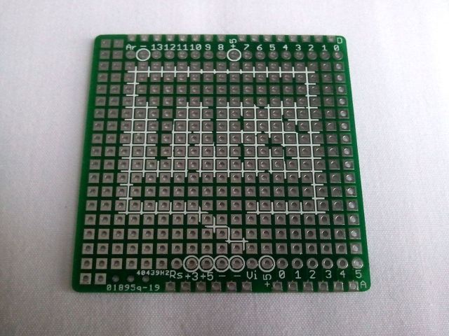
Apparently they clip the silk just fine. :slight_smile: The logo on this card was completely covering the pads on the top of this board.
KhamsaShield-0a.jpg