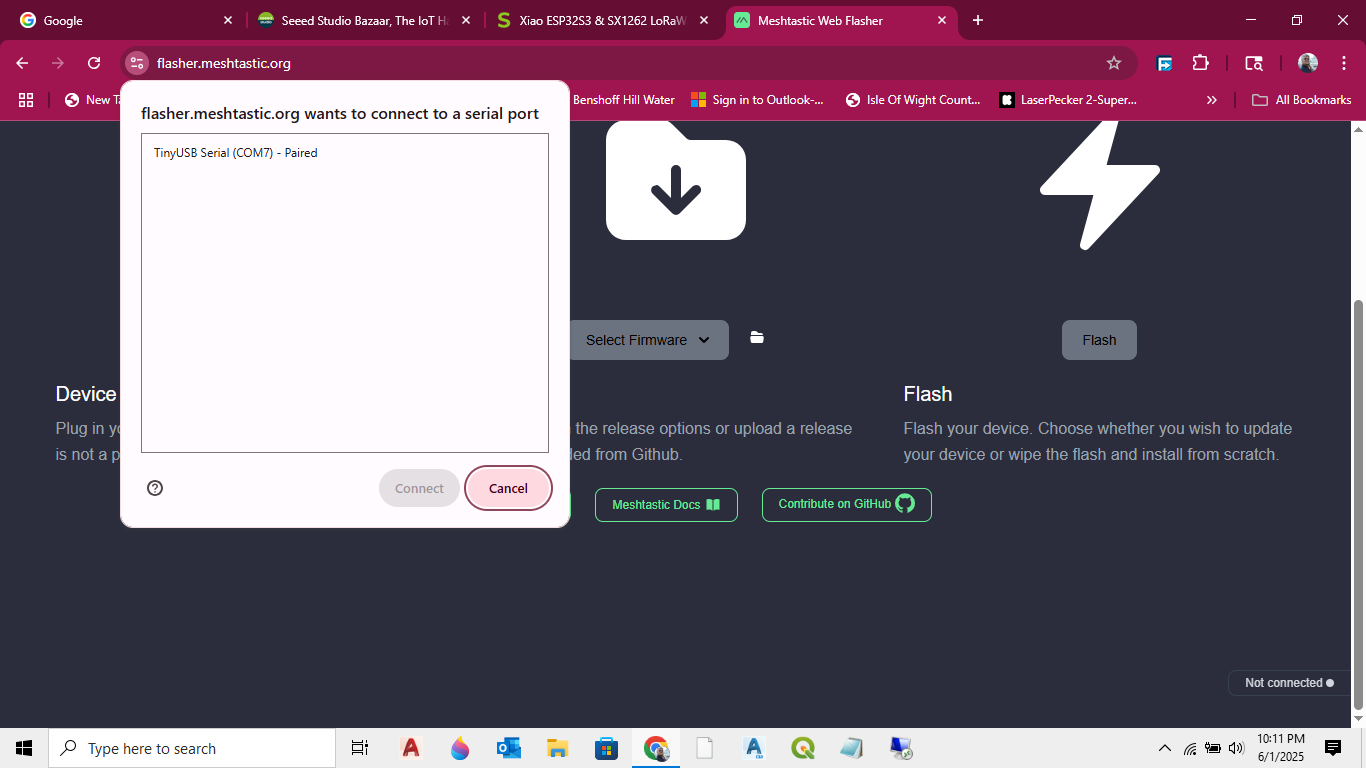
go to website… select serial monitor button… connect device to usb should show as a com port select and see if you are recieving log data… if so you do not need to update firmware… it is running in meshtastic mode
if so you should go to your phone and go to bluetooth and if the device has paired… delete or forget device and re-pair password is 123456 or if it is not set youy will have to look at the serial monitor log and it will tell you the bluetooth random generated pair key
in the future you may want to try to upgrade firmware… but this is not necessary at this time
Hello,
I’m planning to buy a couple of those [Xiao ESP32S3 & SX1262 LoRaWAN] and I’m wondering what are the pins available to connect sensors on it ?
It seems that all the pins are used by the two cards … could you clear my mind ?
Thanx
Prof from France
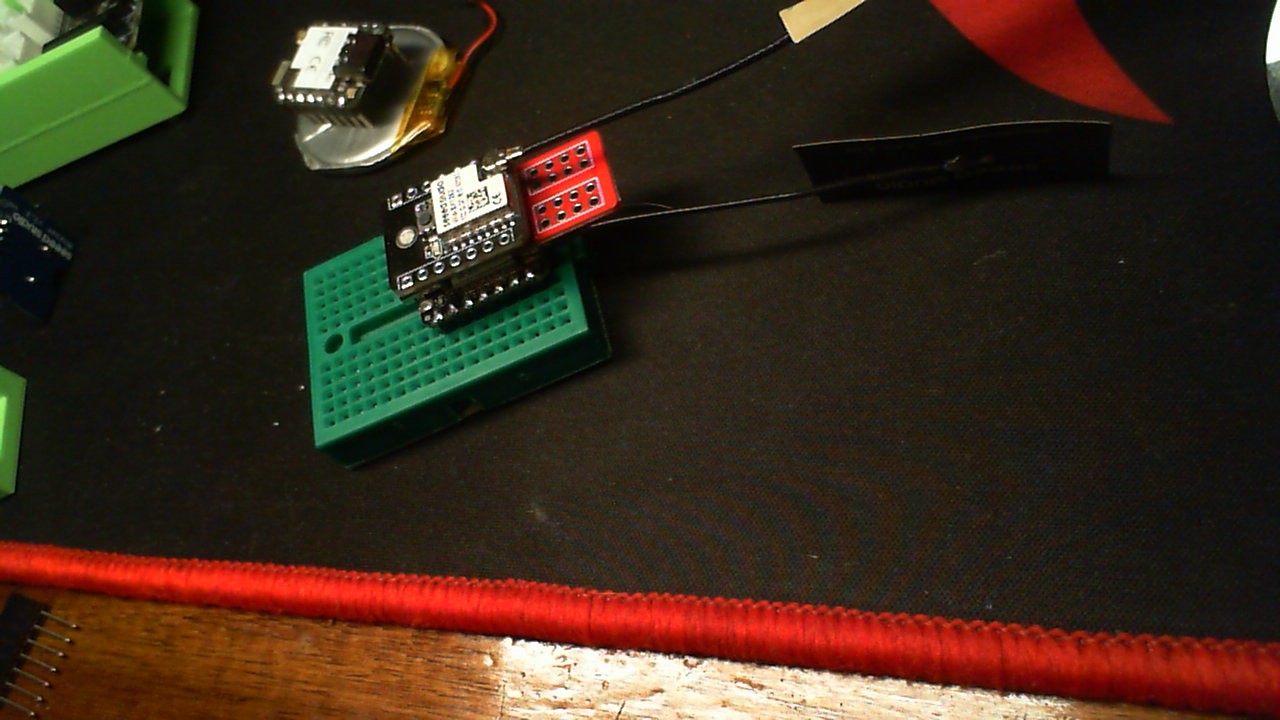
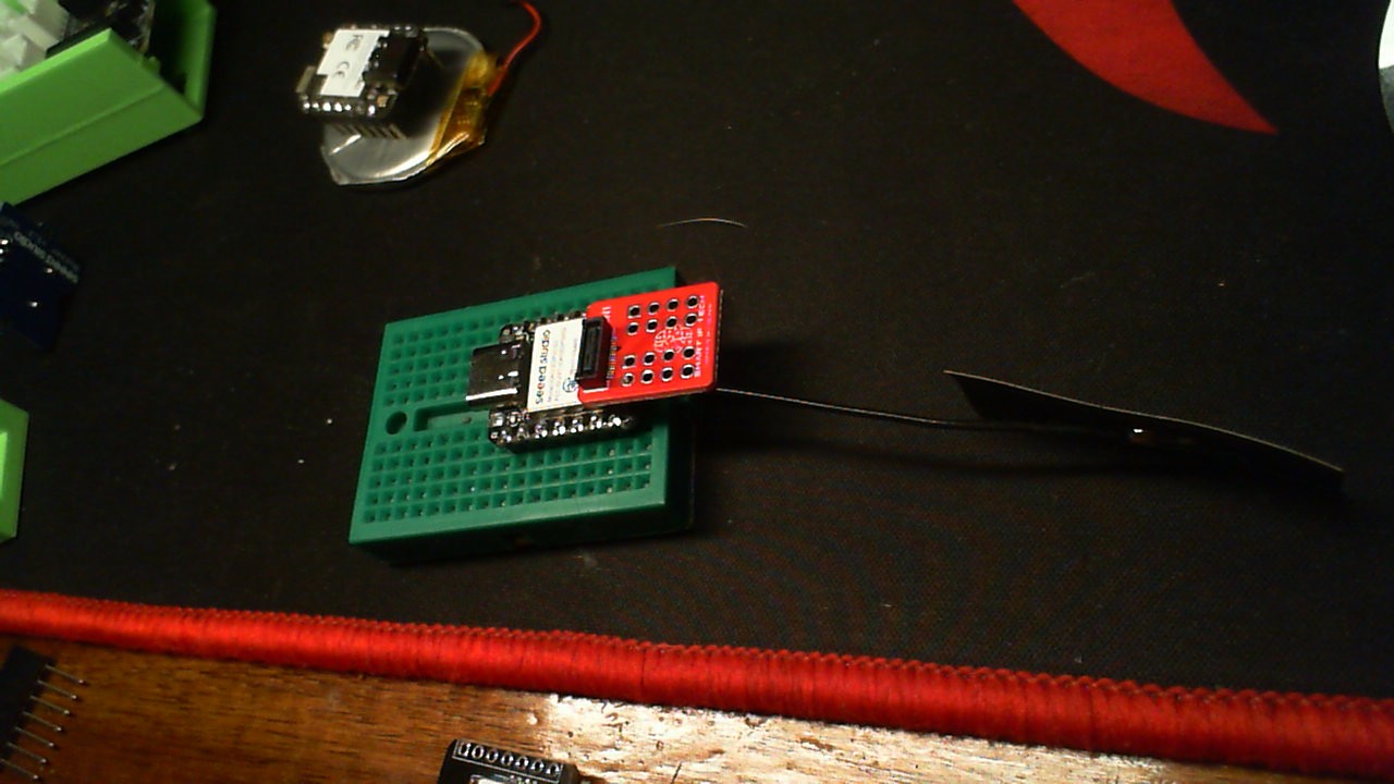
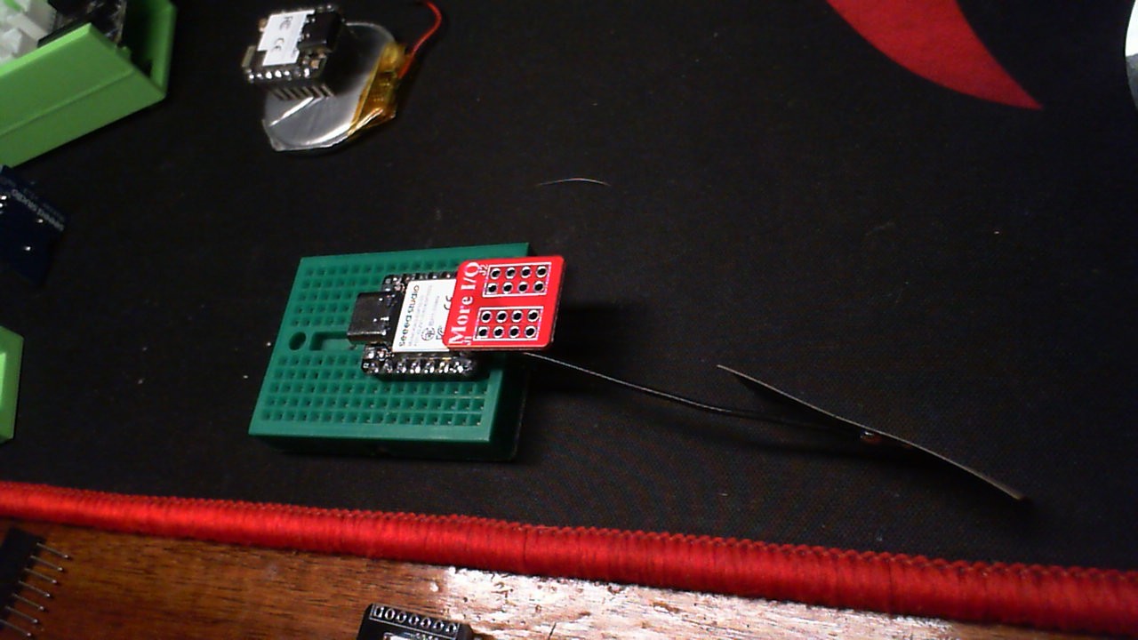
And Welcome Here. There is a schematic available in the WiKi give that a peek also, but the S3 uses the B2B connector for the SX1262 so the other pins are still available, I connected the external buzzer and the I2C ssd_1306 Display in the picture above. The Radio is connected with the SPI interface for example on the Nrf52840 Version So less or No pins are available. The ESP32S3 has more flexibility for that.
Awesome, Please mark @cgwaltney 's post as the Solution So others can find it fast. Thanks for contributing too.
Way to go Sticking with it , when this junk can get confusing as hell…
Yes like he said… it seems the s2 has the most gpio available because it is using the b2b connector leaving the standard XIAO pins availavble… I would also recommend if you are using the s2 device get the XIAO expansion board as well… I mean s3… who can keep up
That is good to know about the green led. So moving on now i have my new firmware. You all talk about using pins so if I up load code (my next thing is to add the little oled screen ) do i just load the coade and the firmware is intact or do I need to see the whole firmware and add code to some part of it.
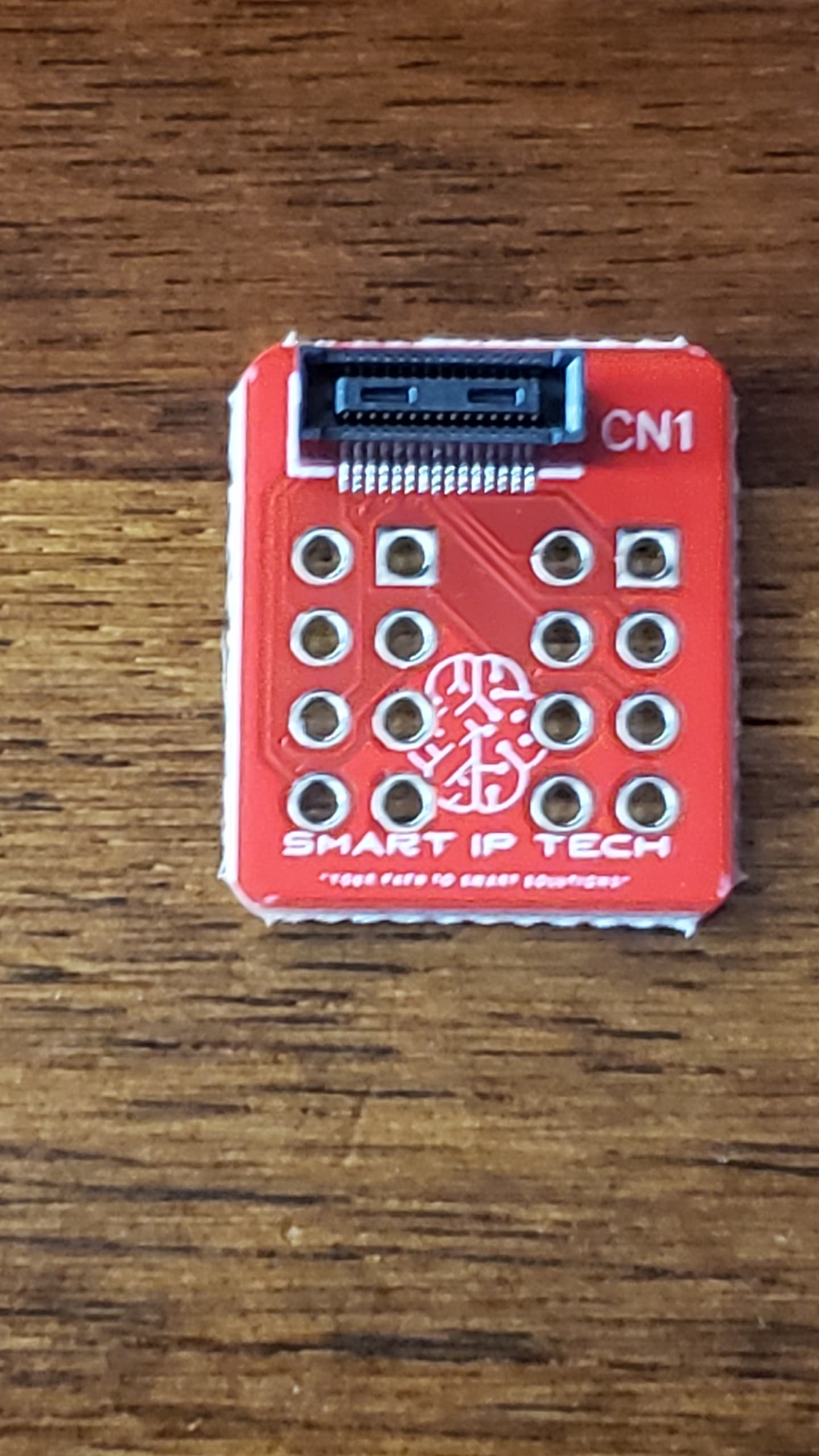
The XIAO ESP32S3 plus board still leaves 10 (ten) pins unused/unconnected on the MCU.
Why not bring those extra 10 pins out as castellated connectors on the bottom edge? (Use 8-layer board if needed)
The PLUS board has extra SMT connectors between the “old” pins, but all the extra pins (except one) gets used up when a LoRA board is plugged in.
EDIT:
Sadly, the SX1261 LoRAWAN cannibalizes the already used D8, D9, D10 SPI bus pins on the ESP32S3plus, where it possibly could have used IO11, IO12, IO13 SPI bus pin on the B2B connector.
In fact, all the connections on the ESP32S3 could have avoided using the small in-between castellated connections in lieu of TWO B2B connectors ON THE BOTTOM, for electrical and mechanical connection.
there is a prototype like that but i dont think it has gone into production… it would probably not be possable for a human to solder those pins without bridging so it is not Maker Friendly
That is why I suggested to keep the 14 thru hole pins, for “makers”, but add two spaced B2B connectors on the bottom, that would replace ALL the small SMD pads on the “PLUS” board. This would give 60 pins to the bottom, more than enough to utilize all the pins, and power.
The “makers” could get a breakout board that has the two bottom 30-pin B2B connectors, as well as the 15 pin 0.1" for bread boarding,
The 0.1" pins could also be used to permanently fix a board, as to not rely on the two bottom B2B connectors.
It is a shame to throw away the opportunity to make the free 10 pins useful.
My board would interface the bottom 60 pins, with my own design.
The design would be used in thousands of boards.
iagree with your comment that wasting pins as NC is not helpful and I agree that handicap makers should not limit the product line… i will pass your comment along…
SO, You may want to read up on the “Concept of Xiao” and did you know you could get a custom Xiao made from the Fusion folks.(including those 2 B2B’s) However You would NEVER be able route all of it… Period!
Maybe do some research more on Why they went the shape, thickness and Size. and also why EVERYONE ELSE copied (ada,robot,Pimorono) You do understand its a 4 layer PCB too… So there’s that.
After a few reply’s you will have enough forum credz to post topics’s feel free. This one is solved, fyi.
I’ll leave you with this,
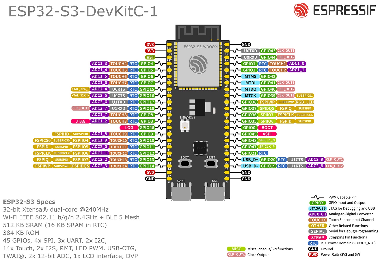
The ESP32-S3 chip has 45 physical GPIO pins, numbered from GPIO0 to GPIO21 and GPIO26 to GPIO48.
Important Notes:
Not all pins are always available: While the chip has 45 GPIO pads, specific development boards might not expose all of them.
Some pins have special functions: Some pins are pre-configured for specific functions like strapping (controlling boot modes) or for accessing Flash/PSRAM memory and are generally not recommended for other uses. (xiao takes advantage of this)
USB-JTAG pins: GPIO19 and GPIO20 are used by USB-JTAG by default. You can use them as regular GPIOs, but this will disable the USB-JTAG functionality.
Highly Configurable I/O: The ESP32-S3 offers great flexibility for connecting peripherals through its IO MUX and GPIO Matrix, allowing you to route peripheral signals to various GPIO pins.
And offer , what is the application? surely Battery power is OUT with that max IO and power regulation would be an issue. Check out the REAL ESP32S3-Dev Kit-1 Dev board … it’s Gigantic
Thanks for your reply.
I have the "XIAO ESP32S3 Plus_V1.0_241025.kicad_pro" file open, and it is clearly 6 layers.
Using 8 layers instead of 6, adds freedom to route traces, and will make it possible to eliminate some vias.
The cost difference is small, I looked at a quote from a major mfg and the difference was $0.075 per board, at a medium size production level.
The bottom B2B connectors could fit 1.) right below the top B2B connector, and 2.) under the USB-C connector.
I have the design files for the board and schematic in front of me, I see no major problems fitting those two connectors, and dropping the extra castellated interfaces.
With bottom B2B connectors there is also a possibility to put other parts on the bottom, memory chip, etc, for more room for vias.
There are three “missing” opportunities for castellated pads between pins 11, 12, 13, 14 that could have been used for SPI MOSI1, MISO1, and SCLK1.
i think the point is the interlaced castlated pins are hard to solder without bridging… making a longer XIAO seems to be a no go with Seeed because XIAO means small in china… they are holding firm on the form factor… breadboard friendly… with minimal exceptions… also if you need all the pins exposed… just buy the dev-kit referenced above… like PJ said… not all pins can be used as some have restrictions… normal castlated pins could theoredically be added to the bottom side… … pads have been added to the underside… but people already cant surface mount solder to them… alot of ideas have been explored… basicly if you are getting to the microscopic level… you can just ask seeed to make you a custom device and do away with the XIAO form factor at all… the product would be embeded into the design and board at thaty point… with that said… we like all the ideas people have and i would like to give credit to Seeed that they will implement alot of the ideas we can back up
Well I say It will NEVER work…But go for it prove me wrong
Power and GND are two, the other four LAYERS are for signals, it will never fit.
You’ll be too thick with 8, and the IO crosstalk will be substantial it will be the noisiest board also. Too many decoupling caps too, Nah it will never work. But Good Luck. just not enough real estate
Really Who’s that? they are pulling your leg…
HTH
GL PJ
I say it’s worthy of it’s own thread, and I’m betting some Seeedineers will chime in also.
The quote for the 8 to 6 layer difference I got from JLC, at 2500 boards, like a $400 order. Check it yourself.
I cannot prove you wrong, else I would lay out the board myself. I’ve done worse.
One 30-pin B2B connector could be placed right under the present one, reusing all those vias. No extra traces.
Breaking out the rest of the pins, not that many, including pins for power and ground. power traces needs rerouting for making space for vias for unused pins.
I like the small size of the board, Dev-kit size is a no-go.
The some eight big test point pad functions, not already in the top B2B, should be relegated to the bottom B2B under the USB-C.
So the extra 30-pin B2B needs 10 for the unused, a maybe the 8 testpoints, (maybe used in factory flashing?) leaving 12 for power, ground, battery.
I have not priced blind-and-buried vias, typically a 300% board cost increase, but should not be needed.
The form factor should be kept along with the standard 14 pins.
Eight layers would not be any thicker, like DDR-4 modules, DDR5 modules have 16 layers.
Yes, OK…Bold statements and some assumptions, Please start Another thread. We will be watching your progress…
GL PJ
Have you done any B2B layouts or boards for Xiao?
I have. However It’s your time , money and dream. Don’t let me dissuade you but technically It’s NOT possible. Unless you have one you can show here.(or in a NEW Thread)
I have made a couple of boards for the XIAO, and I was looking to use the PLUS with the LoRa snapped on, however, the LoRa uses three thru hole pin SPI, that I already have other uses for. The LoRa board could have utilized the other free SPI port.
Why the LoRa didn’t use them I’m guessing that board was older, or used with another product. The pinout on the schematic on the LoRa does not even match pin numbers or sequence of the ESP32S3-XIAO.
I’m already adding a serial 8-bit shift register for the lack of pins, 74LVC595ABQ, but they are not fast enough for emulate another SPI port.
Why Seeed chose to cannibalize the SPI port on the 9, 10, 11 pins, when there is already another free SPI port on the B2B eludes me.
I think two B2B connectors on the bottom would help the maker community, and Seeed.
If I was to design a board for a commercial project, it would be proprietary, unless I got paid to do it.