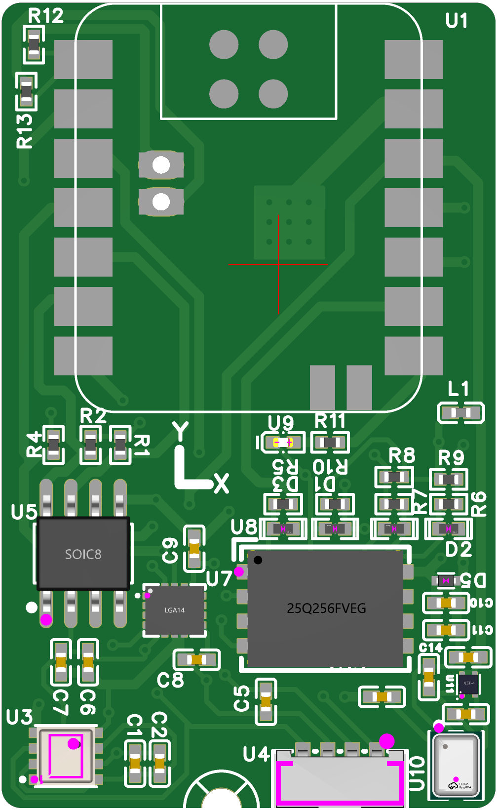
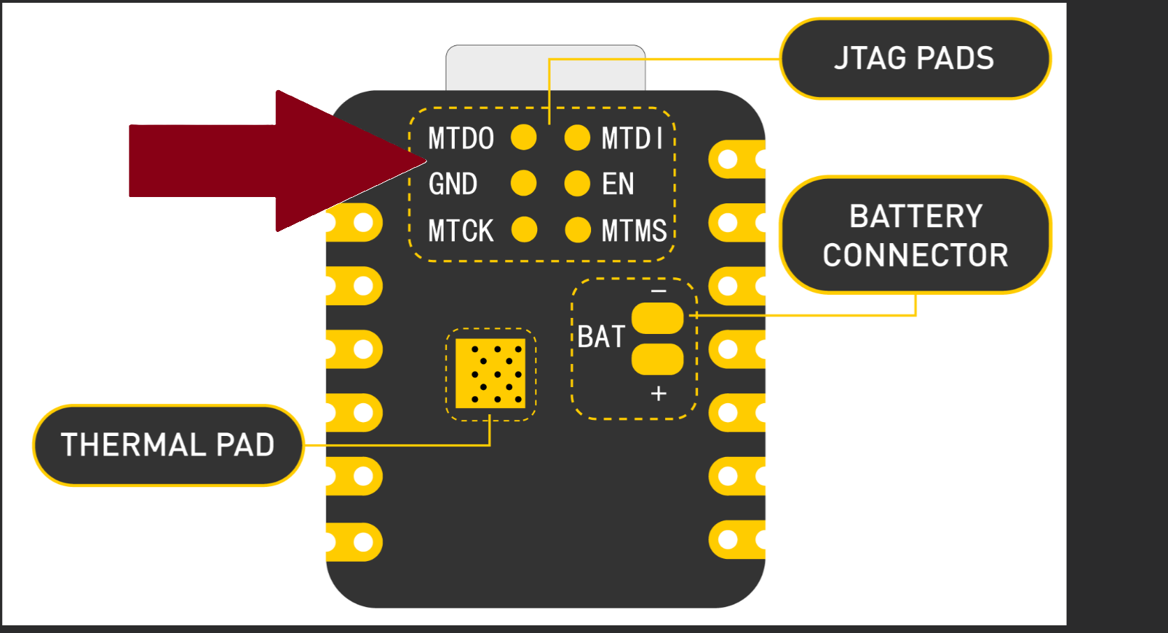
The nRF52 and C3 differ in terms of the presence or absence of thermal pads on the back side, the position of the battery pad, and the holes for the USB connector. Has this been taken into consideration in the PCB design?
To quickly determine whether this is a hardware issue or an implementation issue, I think the best thing to do is to connect the C3 to the PCB with a short wire.
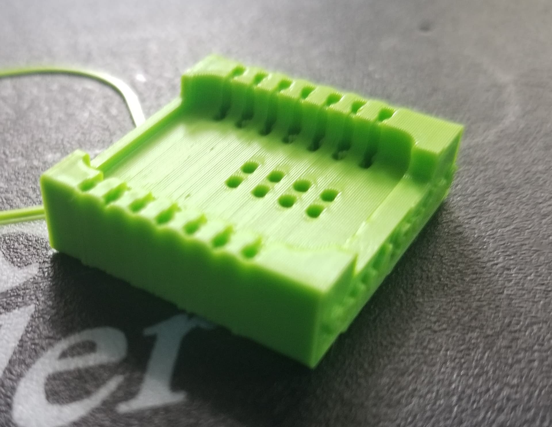
It appears that several ICs are implemented, but are any other than NAND Flash connected to the SPI bus?
Only the sd nand flash is on the SPI bus. Nothing else. Everything else is I2C or analog input.
Here is the pcb pad footprint. I tried to be adaptable to both the nrf52840 and the esp32c3… the battery pads are in the same spot on both Xiao boards (I think)
I said that PJ’s sketch works fine, but there is one thing that concerns me. Pressing the reset button on C3 does not restart it. To restart, I need to reconnect the USB connector(Power on reset?). I don’t know the reason yet.
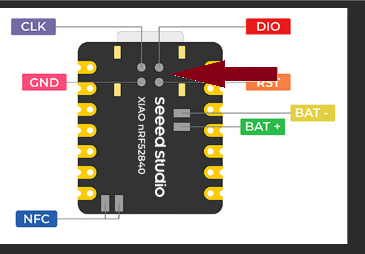
The Reset pin on the C3 isn’t on the bottom like on the Nrf SO I think the pins are being shorted a little on PCB of on the footprint for one vs the other if that makes sense.?
on the dev board the reset only works for me on the NRF’s none of the ESP’s btw ? I put a piece of thin business card between the pogos and the ESP’s , try that and press the C3 reset should work.
HTH
GL PJ
I vote lift one up and test again…
It looks very nice too the PCB ,
yes they are indeed, However the four (4) points vs the six(6) I think they are overlaping (shorting) on the C3 and landing in the middle of two.
I maybe all wet… ?
but if you unsolder one and put pins on it , only connect the power and SD test that. ?
MISO=GPIO9 seems to be deeply related to the fact that it is a strap pin. For example, in sketches that do not use GPIO9, such as I2C_Scanner, the device restarts normally when the reset button is pressed.
EDIT;
This sketch uses D3 (GPIO5) for MOSI instead of strapping pin D9 (GPIO9). I was able to restart using the XIAO reset button.
The problem with @NRav90 may be caused by the strapping pin. If you want to try changing MOSI=D9 (GPIO9) to another pin, please refer to the attached sketch.
To restart XIAO ESP32C3 with the reset button, the strapping pin (D9) GPIO9 must be set to HIGH. GPIO9 is used as MISO of SPI bus, so even if it is pulled up, if the NAND Flash outputs LOW, GPIO9 will become LOW, and it will not be possible to restart with the reset button.